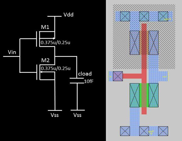
……..(sentence continued from above image) the above image is the waveform from SPICE simulation of inverter ‘extracted’ from above layout (MAGIC is a layout tool which has a feature to extract the SPICE netlist.. Stay tuned, and I will tell you
how)
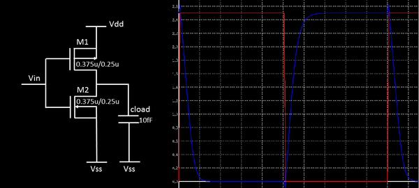
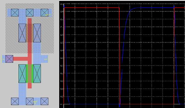
The waveforms of ‘zero’ wire size CMOS and ‘finite’ wire size CMOS looks so identical. This proves that the layout is functionally correct. But…..if you closely look into the delays of the inverter, its 58ps for ‘zero’ wire size CMOS and 68ps for ‘finite’ wire size CMOS. There is roughly ~10ps difference in the ‘drawn’ inverter and ‘fabricated’ inverter. That’s the key. Imagine a
series of 100 such inverters on a chip. The cumulative delay difference in the inverter chain between ‘drawn’ and ‘fabricated’ will be approximately ~1000ps i.e. close to 1ns. That’s huge!! And hence, we need to understand, how ‘real’ is different from ‘drawn’
I am happy to announce that this will be the topic of my next course (not published yet) which will be called as “VLSI Academy –
Design rules and custom layout”. This course will mainly focus on design rules needed for fabricating a design onto a chip, subckt design and an application design, namely SRAM.
‘New’ is always exciting….So stay excited, while I am getting ready to take you all to a world of layouts, and show you, how its so related to Static timing analysis
Happy Learning !!
FYI:
First of all, Thanks a lot for being a part of this wonderful community, where you will find a bundle of knowledge sharing
and improve your analytical skills.
Secondly, as you might be aware (from my announcements), that we are going deeper and deeper into projects, rather than just theory, and hence will be introducing Lab and Layout courses (mostly open-source) for you to install and practice what you have learnt in all my courses.
But before that, I would need you to at-least have completed the below courses and be ready for labs, as the concepts are really very important. Physical design flow theory and labs will be incomplete without deep knowledge of every aspect of it. If you have already taken the courses, you can safely ignore this message.
For others, here’s you chance to get the below courses for $11. This offer is valid till tonight 7th June 11:59pm IST. Make sure to take fullest advantage of these courses and be prepared for Labs and Layout
Static timing analysis:
Circuit design and SPICE simulations – Part 1:
Circuit design and SPICE simulations – Part 2:
Clock tree synthesis – Part 1:
Clock tree synthesis – Part 2:
Signal Integrity:
“Good things come in small packages”
So get hold of
each package to observe good things J …. Happy Learning !!