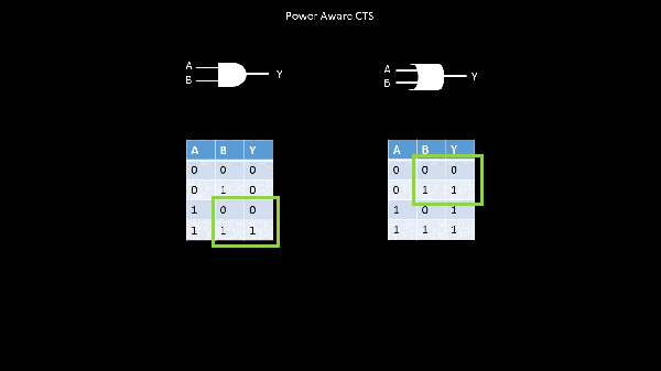
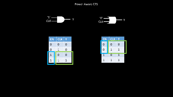
So, I will call one input of the gates as 'EN' i.e. enable signal, and the other one as 'CLK'. In case of an 'AND' gate, whenever 'EN' is high, and in case of OR gate whenever the 'EN' is low, the output 'Y' is 'CLK'
With these basics in place, next step is identify functionality for those parts of your chip which
remain silent or do not function while another part of your chip, which functions. If we are able to isolate these parts, we can combine that with above concepts and come up with a clock network which will potentially save huge power, in turn, which will help you save some battery on your mobile phones.
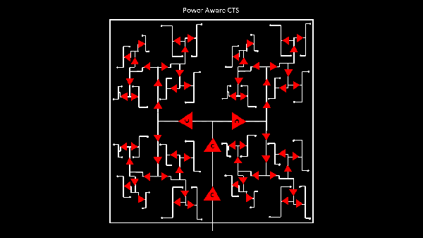
To nail the bigger picture, I will use the below small one to explain, what I mean by above statement