Power aware clock tree synthesis - Part 4

Published: Tue, 10/13/15

Hi

We were looking for a solution for below scenario, and you will be amazed to see, how an 'Universal Gate' solves the below problem (of-course, at the cost of increased area, but you save lot of power, which is a prime necessity in your smartphones)

The question is 'How'? Let's go back to school and recollect 'We can build any gate using NAND/NOR gate, and hence they are called "universal gates"'


So a buffer can be reconstructed something like below....

....OR gate becomes something like below....
.....and finally AND gate becomes like below
I have solved 50% of the problem. The rest 50% lies in plugging the right kind of gate (using NAND gate) at below right place
And there you go, you plug the right logic and achieve things needed for a 'zero skew' clock tree network, while saving immense amount of power
You might think, we are adding a lot of area into the design. But think of a clock tree network that was huge enough like below. Using this simple and effective technique, we save almost half of switching and short circuit power

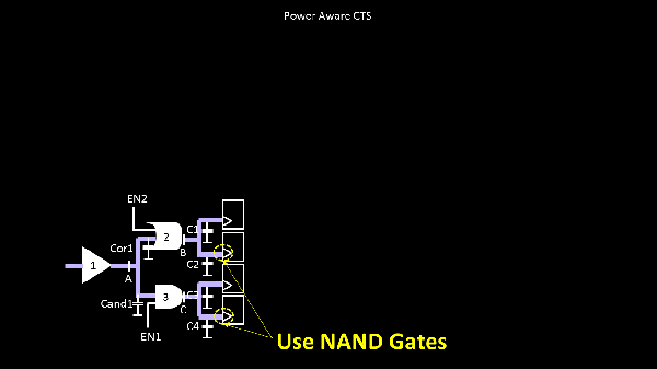
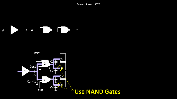
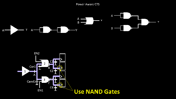
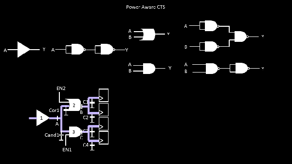
There's a famous saying by Benjamin Franklin "A penny saved is a penny earned"


In a VLSI world, I believe, this applies for power as well :). And, that's the reason, you see a tremendous research happening in this field. 


If you are a PhD, looking for research topic, I bet you, this is a good one


Happy Learning !!

Kunal (http://vlsisystemdesign.com/)

FYI : Are you ready for next VLSI interview rounds? If not, step up and get back to work using below courses and let know on the forum if you face issues/doubts. We would be happy to help

Circuit design and SPICE simulations:

Physical design flow

Clock Tree Synthesis

Signal Integrity

VLSI - Essential concepts and detailed interview guide