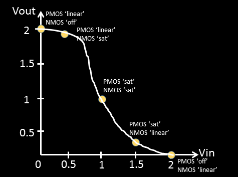
With that introduction, let me first show you (and most of you might already know), the above curve is derived (using well defined steps) from NMOS/PMOS Id-Vd curves. Now, is that surprising? Well, 'yes' and 'no'. Why 'no'? Because, CMOS is built using NMOS/PMOS, so obviously, it will have connection with their
characteristics
Why 'yes'? Because, what I have showed you, till now, through my videos or posts, is the, NMOS/PMOS drain current (Id) and drain voltage (Vds) characteristics based on constant gate-voltage (Vgs), but the above curve is completely dependent on 'Vin' and 'Vout'
That's the catch!!! There should be some way to convert 'Vds' and 'Vgs' as function of 'Vin' and 'Vout'
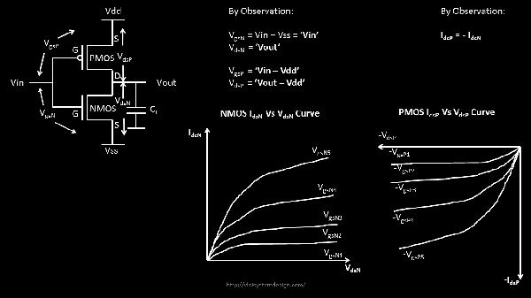
Let's start with basic NMOS/PMOS curves, which I believe can
easily be derived using SPICE simulations. Below image also shows the relationship between different 'transistor' level voltages (i.e. Vds, Vgs) and 'logic gate' level voltages (i.e. Vin, Vout)