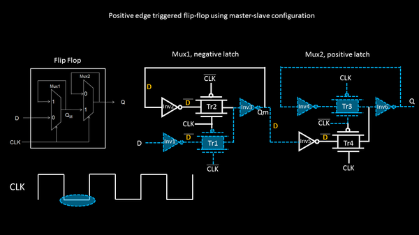
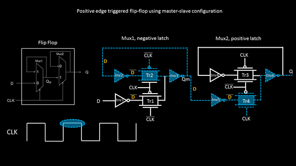
Clk-to-q delay, library setup and hold time - Part 2

Published: Sun, 04/05/15

Hi 

This is in continuation to the previous post, where I explained about transistor level implementation of negative and positive latch. In this post, I will showing images on transistor level implementation of flip-flop and finally, we will nail down the 3 terms i.e. clk-to-q delay, library setup and library hold time.

Lets begin with the interior of flip-flop

When CLK is 'low', “Tr1” and “Tr3” turns ON. Hence, input 'D' is latched to output 'Qm' of negative latch.

'Inv4, Inv6' holds the 'Q' state of slave positive latch

Also, D_bar, is ready at output of 'Inv5', to propagate till 'Q', when CLK becomes 'high'

Setup Time is the time before rising edge of CLK, that input D become valid i.e. 'D' input has to be stable such that Qm is sent out, to Q reliably

Input 'D' takes at least 3 inverter delays (Inv1, Inv3 and Inv5/Inv2) + 1 transmission gate delay (Tr1) to become stable before rising edge of CLK

Setup Time = 3 Inverter delay + 1 Transmission gate delay 

When CLK is 'high', “Tr2” and “Tr4” turns ON. Hence, input 'Qm' (which is 'D' input from previous 'low' CLK) is latched to output 'Q' of negative latch, through 'Tr4' and 'Inv6'

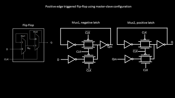
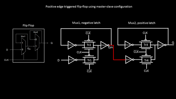
'Inv2, Inv3' holds the 'Qm' state of master negative latch

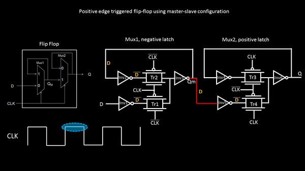
Clk-Q delay is the time needed to propagate 'Qm' to 'Q'. Note, that 'D' (or 'Qm' from low 'CLK') was stable till output of 'Inv5'. So the time required, to propagate is 1 transmission gate delay + 1 inverter delay

Clk-Q delay = 1 transmission gate delay + 1 inverter delay


Hold Time is the time for which 'D' input remain valid after clock edge. In this case, 'Tr1' is OFF after rising 'CLK'. So, 'D' is allowed to change OR can change, immediately after rise 'CLK' edge. So Hold time is 'zero'

Hold Time = 'zero'

And here we go, we just beat the dead horse down :)

I would request you to post some comments/feedbacks/doubts on this post.

Thanks

VSD Team (http://vlsisystemdesign.com/)