Hi Everyone, who's been a part of physical design or STA, must have definitely gone through this. When I thought about it, like 5 years back, as a fresher, I really wished, somebody could had
explained me this one in a much better way, with images. I believe "A picture is worth a thousand
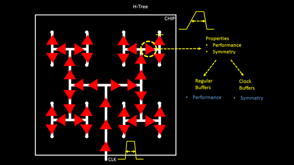
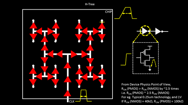
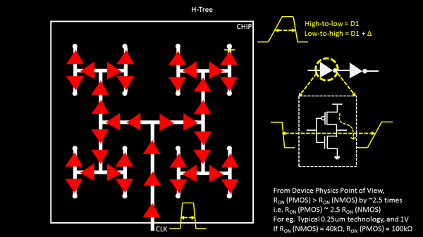
words" :) Never mind, I understood the topic and created few images on my own. It becomes relatively simple to understand it this way. So the problem is the asymmetrical waveform, that you can get at clock endpoint, as shown below. We really (most of the time) donot want to see these
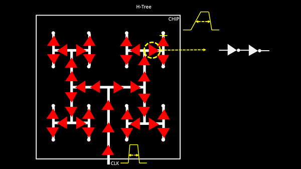
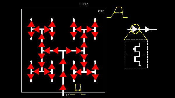
wave-forms in clock network, as its the most critical section of the entire circuit. (donot worry about the complicated circuit below, its a clock tree)
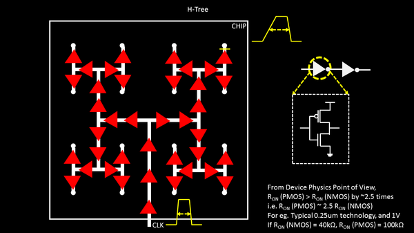
Let's try to look into this one from NMOS/PMOS resistance point-of-view, like below If we look resistance from device physics sense, the resistance of PMOS transistor is typically 2.5 times of an exact size NMOS transistor. I will prove this from SPICE
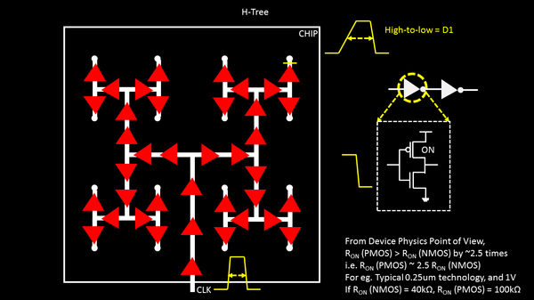
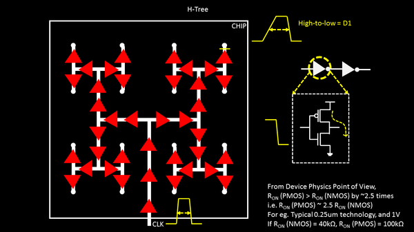
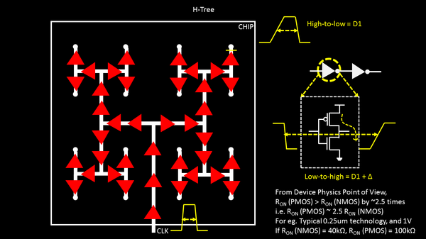
simulations and some concepts, later, in my video lectures. So, for 0.25 micron technology, for eg., if R(NMOS) = 40 k-ohm, then R(PMOS) ~ 100 k-ohm. So, if high-to-low delay is D1, then ...... (sentence continued after below 3 images) (above sentence continued....) then low-to-high delay is D1+delta, because, same size PMOS (which has a higher resistance than NMOS), takes more time to charge the
output load So now, we know the crux of the problem, i.e. high-to-low delay is not equal to low-to-high delay And, so we are seeing that ugly waveform, at the clock endpoint, with
un-equal rise-fall times. But, hey, good news, we have a solution to this problem. We will
follow what Abraham Maslow quoted in Toward a Psychology of Being. "I suppose it is tempting, if the only tool you have is a hammer, to treat everything as if it were a nail" Let's nail this one in the next post :) Thanks Kunal
(http://vlsisystemdesign.com/) |
|
|