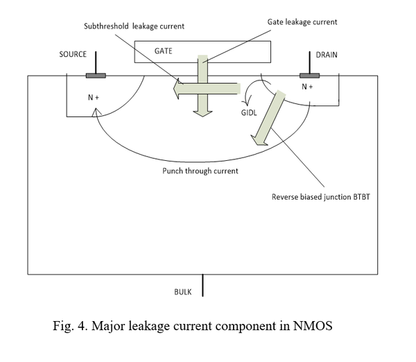
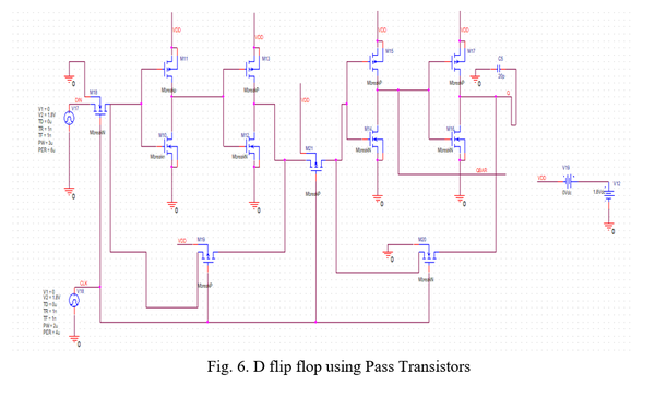
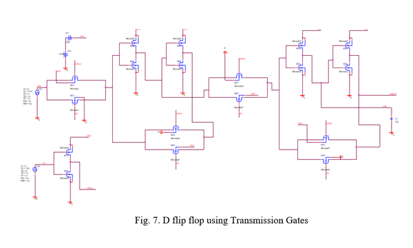
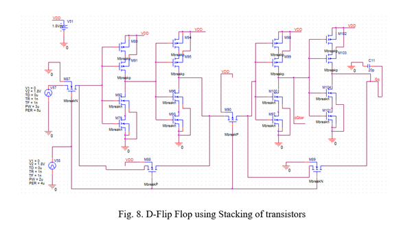
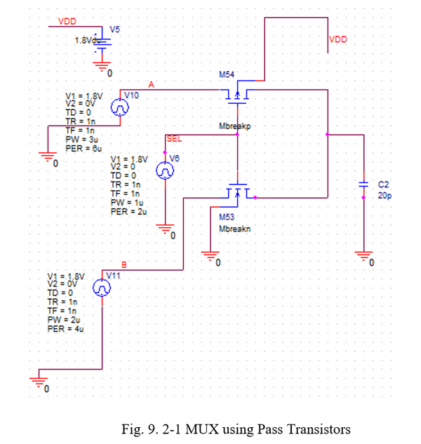
3. LEAKAGE POWER DISSIPATION
(i) SUBTHRESHOLD LEAKAGE POWER DISSIPATION
When gate voltage is less than threshold voltage of MOSFET then even a current flow from drain to source through channel because of drain voltage (VDS) this current is called as Subthreshold Leakage Current as shown in “Fig. 4”. It causes dissipation of power known as subthreshold leakage power dissipation.
(ii) GATE-OXIDE TUNNELING LEAKAGE POWER DISSIPATION
In short channel devices, resultant of electric field of gate voltage electric field and drain voltage electric field causes electrons to move in zig zag manner and some electrons which gain extra energy at pinch off tunnel to gate through insulating SiO2 layer. This gives to gate leakage current towards substrate as shown in “Fig. 4”. It causes dissipation of power known as gate oxide tunnelling leakage power
dissipation.
(ii) REVERSE BIASED JUNCTION BTBT POWER DISSIPATION
It occurs when the source or drain of an NMOS is at VDD or in case of PMOS is at ground. Reversed biased PN diode is formed at source or drain of transistors causing flow of current through substrate as shown in “Fig. 4”. In this process tunnelling of electron of p type substrate from valence band to conduction band of n type drain occur. Hence, this current is known as Reverse Biased Junction BTBT Current. It
causes dissipation of power known as reversed biased junction BTBT power dissipation.