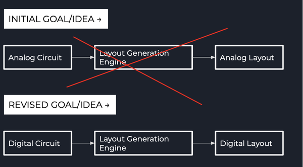
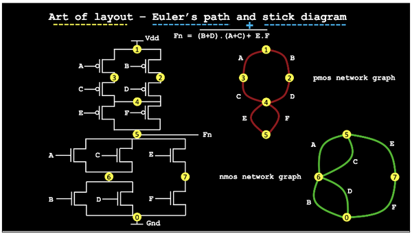
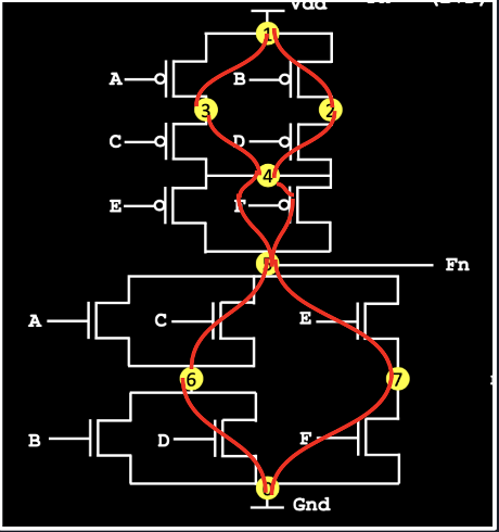
The Problem -- (Circuit to Layout Conversion)
No. of Foundries → TSMC,GF,Intel,Samsung, UMC etc. As the technology scales down, all these foundries release
their versions of PDK and these PDKs are different for different foundries.
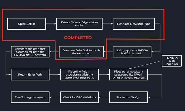
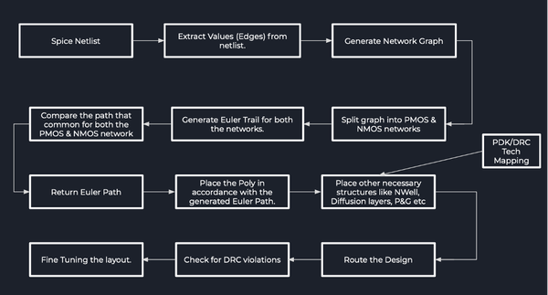
Standard Cell Layout Generation → Characterized Std Cells are required for the PnR process. Every time the tech node
changes, the Char. Engineer/Layout Engineer has to draw the circuits for the basic std cells and lay it out individually. This is a time-consuming process. (Given the exorbitant no. of cells ). The idea is to automate the std cell layout generation for various std. Cells.
Existing Projects (Active) --
ALIGN → (Analog Layouts Intelligently Generated from
Netlists) -- This is a collaborative project by UMinn (Sachin Sapatnekar), TAMU and Intel Labs, Oregon funded by DARPA. (https://github.com/ALIGN-analoglayout/ALIGN-public)
MAGICAL → (Machine Generated Analog IC Layout) -- This is a
collaborative project by UT-Austin (David Z Pan) and is financed by DARPA. (https://github.com/magical-eda/MAGICAL)