My name is Ashutosh Sharma. I wanted to share the learnings of my eight weeks summer internship in 2020 at VSD Corporation. So, here is my journey of thoughts and processes which happened with and within me. I hope you find it insightful.
I worked as an Analog IP Design Intern at VSD Corporation. The experience which I got under Sir Kunal Ghosh was very delightful. During the eight weeks, I practiced the process of doing research extensively. After performing it, I became more confident to work out any given research problem statement.
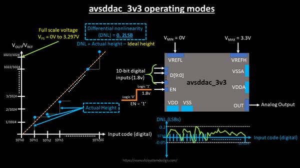
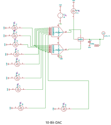
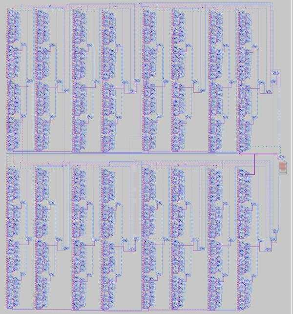
This research internship program was for eight weeks with a sequential six-staged format. My assigned objective was to design a 10-Bit Digital to Analog Converter using osu180nm tech node and open-source EDA tools.
The specs were on the VSD corporation website. The first week’s task was to research the given topic. So, I read about the given topic through various sources. I got some idea and then thought of reading the three chapters related to ADC and DACs from CMOS: Circuit Design, Layout, and Simulation, a book by R. Jacob Baker. By this, I got to know many things associated with DACs.
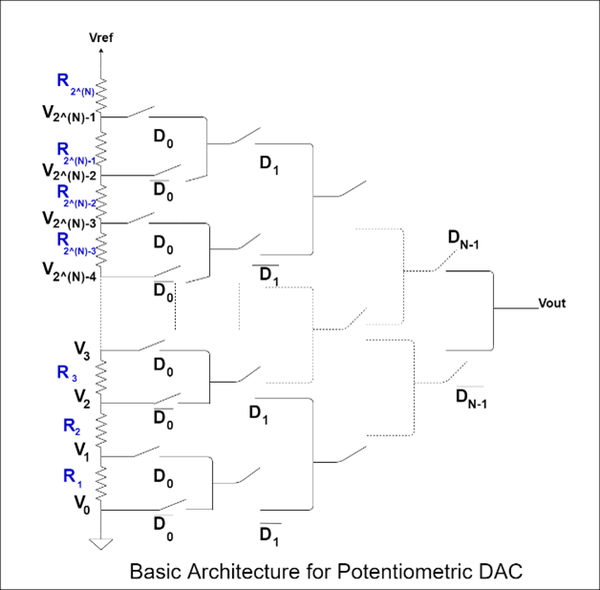
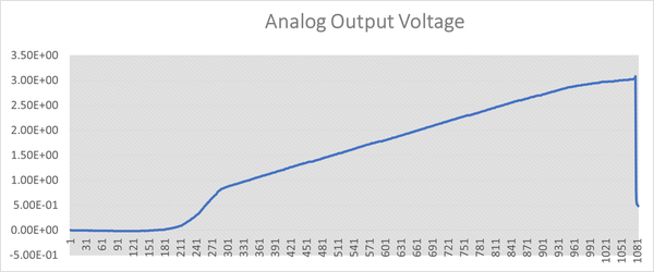
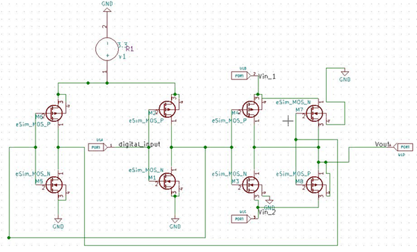
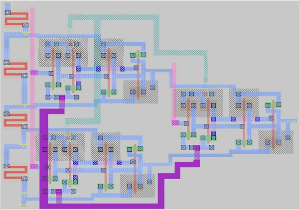
The basic idea, which I understood in DAC is to divide the voltage into N different voltage values in the range of Vref+ and Vref- for an N-Bit DAC. The design I used to achieve this is the simple resistor string DAC which consists of resistors in series. These resistors are then connected to various switches in such a fashion that it routes the exact voltage to the output.
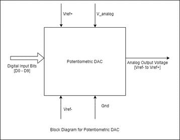
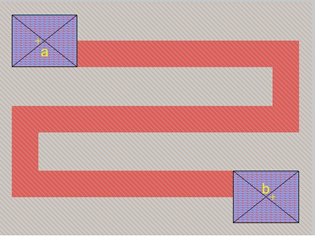
Have a look at the simplified architecture for potentiometric-DAC given below.