As asked by many of you, below is the registration link for Advanced Physical Design Workshop using OpenLANE/Sky130 (expires tonight in 12hours):
Anybody with even a small presence in the semiconductor domain would have heard about Google-SkyWater’s latest announcement of making the first manufacturable open-source 130nm public and with it would have acknowledged the massive door of opportunities that this announcement has opened. And it was almost around that time efabless conceived the
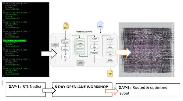
OpenLANE flow – a completely automated RTL2GDS flow. Now that’s SOMETHING!
These developments have now bridged the very gap that had existed in the Open source ASIC Digital Design for long, namely, that of a foundry-grade PDK and reliable EDA Tools.
We at VLSI System Design (VSD) Corp. Pvt. Ltd. are always focused at delivering industry-level workshops with latest resources that are available out there and the blogs here (https://www.vlsisystemdesign.com/blogs/) are strong testimonies to that. So with the announcement of Google-Sky130 PDK and Openlane we are glad to present a full-fledged 5-day workshop on Advanced Physical
Design using Openlane/Sky130.
“Can I build a chip of my own?”
“What are these challenges?”
“What is the process?”- If you have these questions and if you are eager to delve into the world of ASIC design flow, then this is the workshop for you!
The reason being, this workshop is so designed that anyone with just some basic idea about Physical Design flow will be able to fully understand the entire ASIC Design cycle ( and with some effort can build a chip from scratch too). Also, the objective for each day of the workshop is structured in a way such that one can refresh the basics while
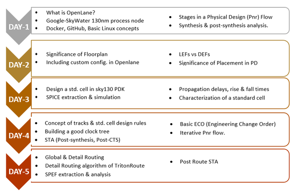
gradually building on advanced concepts. Below is a little sneak-peek of the objectives for each day: