Hi
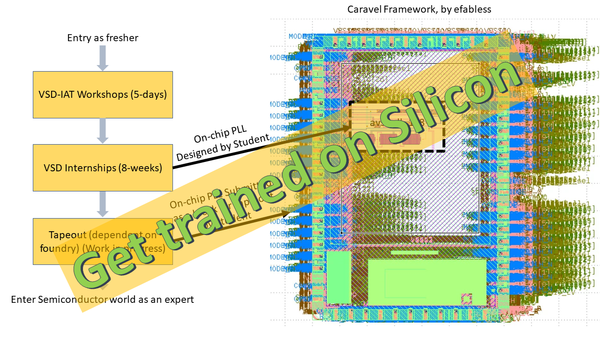
Just last week, one of our VSD Interns released a PLL chip for production at Skywater Fab through efabless Caravel process. And above image summarizes the whole process. Not only that, but there are also 32 more VSD interns who went through 2 out of above 3 stages and have done terrific work in their 8-week internship
program. Their chips are almost ready for production.
More importantly, VSD interns exactly know how VLSI industry works and accordingly either preparing for interviews or approaching right profiles
Can you imagine, a student with minimal knowledge and experience about VLSI and semi-conductors, getting an opportunity for producing chips (called as tape-out in industry)? Well, it is not that easy as it sounds. There is lot of technology that runs behind the scenes and we call it VSD-IAT (Intelligent assessment technology)
Now, would you like to experience the whole process? Well, we are just getting started for 1st Advanced Physical design workshop and internship for 2021. Below are the details. Note important dates
Workshop + internship important dates:
1week workshop using OpenLANE/Skywater 130nm PDK’s (22nd – 26th January 2021)
1week for Git resume (27th – 31st January 2021)
8-weeks Research IP design internship using Sky130nm PDK’s (Starting 1st Feb 2021, only for participants who successfully complete above workshop, with a valid Git Repository)
Workshop details:
https://www.vlsisystemdesign.com/advanced-physical-design-using-openlane-sky130/
FYI – For previous OpenLANE/Sky130 workshop participants, who have successfully submitted their GitHub links, we will email you internship details
Join the workshop/internship and experience the process. I can guarantee you; these 10-weeks will entirely change your perception about VLSI, Semi-conductors and in general, towards LIFE
All the best and happy learning