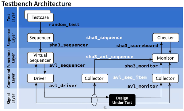
Let me show you a basic testbench architecture (We have taken SHA3 core as an example to explain the architecture in webinar)
First, we have sha3_sequnce, which is basically the input string. Then we have sha3_avl_sequence which is basically splits the string into “200 bytes each”, with “zero padding” depending on “modes”. And finally, at the
“avl_driver” level, we are converting all these into “avl transaction”. Hence above terminologies in the rounded square boxes, is what UVM uses.
If you are creating a sequence, you call it “sequencers”. If you are converting one sequence to another, you are not creating, but you are mapping data into another sequence, from one sequence to another sequence. This is called as “virtual sequencer”. This is where we will be splitting
the original sha3 string input into multiple frames.
Finally, the whole sequence needs to be split into multiple sequence items and that’s the work of a driver, to drive that to verilog input (Design under test)
So, it does look like a generic diagram of a testbench, isn’t it?
I am very sure, there is an inherent curiosity to learn more about sha3 core and the terms highlighted in above explanation of testbench architecture
Learn more about it in the upcoming online webinar “Opensource Verification and Emulation using Embedded-UVM” on 15th June’2019 9am to 1pm IST. Here’s the registration link: [Ticketing closes in 43hours]
http://go.eventshigh.com/wnako
Make sure you complete your assignments given during the webinar and earn certificates, which can be potential value addition for your VLSI verification interviews
All the best and I will see you LIVE on 15th June