Want to protect your transistor? Meet TIE-HI cell

Published: Mon, 04/10/17

With its very few connections and a relatively simple circuit, tie-hi cell is found to be one of the most important place in IC design, thus protecting all your logic gates from the spurious disturbances happening at VDD, normally called as ‘voltage droop’
The general idea is if you know or intend to provide constant logic ‘0’ or logic ‘1’ to any inputs of your gates (for tie-hi, its logic ‘1’), then refrain from directly connecting it to VDD, instead add a tie-hi cell in between VDD and gate static input. Let tie-high receive the VDD and provide a clean output of logic ‘1’ to static input of gate. And there’s proof, that any disturbance in power or VDD line will just be filtered out at output of tie-hi cell, thus protecting your gate oxide from damage
Here’s how your tie-hi cell interiors look like:
You see the connections for NMOS transistor ‘M1’. It forms a strong reverse biased diode whose output goes to PMOS transistor ‘M2’. Now here’s the puzzling waveform at the output port
In all the above text, I was mentioning above a clean, distortion free logic ‘1’, so does the above blue waveform at output contradicts what I mentioned above? No, it doesn’t. The range of distortion is very less, somewhere in pico-volts. Now, what really matters is the distortion in the power supply line, and see the waveform at output port.
Let’s take a worst case scenario, where we distort VDD line, and below is what we see:
The ‘red’ waveform at 1.8v is the power supply distortion, famously called as voltage droop. And the ‘blue’ waveform is what you see at the output of tie-high cell. Looking closely at the VDD and tie-hi output, it appears to be something like below:
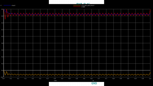
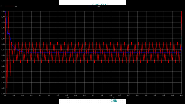
Now this VDD distortion is on the range of 70mV which is enough to damage ‘gate oxide’. But the variation at the output of tie-hi cell is minimal and so it’s the tie-hi that protects your gate oxide and hence the entire logic cell from being damaged.
Similar functionality and simulations can be derived for tie-low, I will leave that analysis to you….
Now the role of tie-hi reminds me of a wonderful quote from Martin Buber, “All journeys have secret destinations of which the traveler is unaware”. And so is the journey of tie-hi cell!!
To learn more about tie-hi cell, its behavior or something more about ‘unsung’ heroes of IC design, register to my courses using below discount links, which is valid till tomorrow i.e. 11th April mid-night 11:59pm IST: Till then, happy learning!!!            

Library characterization and modelling – Part 1:

Static timing analysis – Part 1:

Static timing analysis – Part 2:

Physical design flow:

Circuit design and SPICE simulations – Part 1:

Circuit design and SPICE simulations – Part 2:

Custom layout:

Clock tree synthesis – Part 1:

Clock tree synthesis – Part 2:

Signal integrity:

VLSI – Essential concepts and detailed interview guide: