Are you finding CCS timing complicated?.....Not anymore!!

Published: Sun, 02/26/17

All you need is a right guidance and right strategy…..
Well, from the day I was involved into complicated STA analysis for full chip with almost 150M+ instance count design, I had been getting a lot of questions from my colleagues regarding CCS timing…like, they find it difficult to understand the CCS timing format.
From that point onwards, I already had few notes on CCS timing, and I find this is the right course and place to collate all notes that I had and give it you..Below is the complete pre-launch course on “Library characterization and modelling – Part 1”….The below coupon link is valid till tomorrow mid-night i.e. 27th Feb, 11:59pm IST
It all starts with what you have on your plate. Below image shows what you exactly have (All below waveforms are based on SPICE simulations using ngSPICE. Make sure you complete my course on “Circuit design and SPICE simulations”)
We have input slew, related_pin, output load and output switching current waveform for a buffer. Its very easy to get the above and all you need to do this is write SPICE netlist for the buffer, add input stimulus, output load, and necessary power/ground sources. I have all these steps clubbed in a course on “Circuit design and SPICE simulations”
Once you have all them, we try to put it in a reasonable format. It says, for a specific input slew, and a specific output load, the rising current at output node is what you see above at out_1 pin, and below is the table to put it in
The current waveform that you see for a specific input slew and output load is a vector i.e. a range of values, that represents the current waveform. What an EDA tool for STA needs to do is extract the right voltage waveform from the above current waveform and compute the delay. People ask me why do we go for CCS timing models if it’s so computation expensive. Well, I do not see a more accurate way to compute delay for advanced nodes other than CCS (and ECSM, which will be introduced later)
The above is a one input slew and one output capacitance combination. We have similar output current waveforms for all combinations of slew and load, and below is how the table will look like:
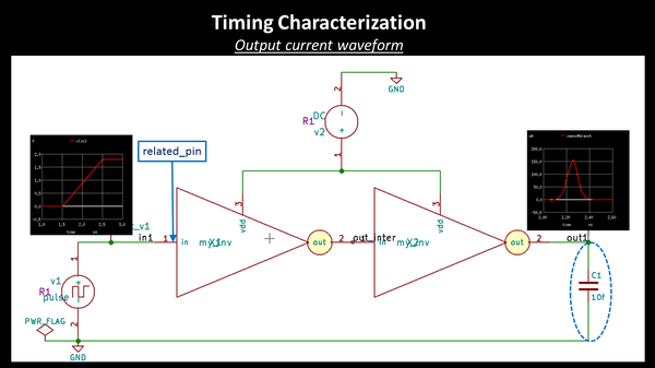
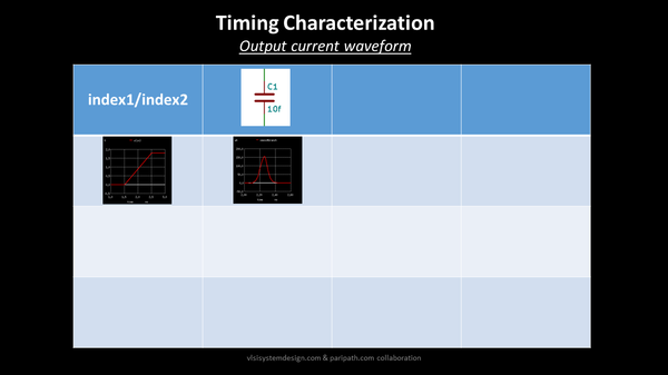
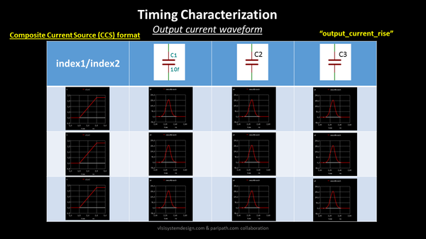
Next job, is to interpret the exact syntax and semantics of CCS timing format, which I don’t think will be a difficult job anymore. I would still be covering that in my course on “Library Characterization and modelling – Part 1” course.
So, do you still find CCS timing model a complicated one to understand?
Just as Oli Gardner says “The customer isn’t always right. But if you don’t listen to them, your product won’t be either
I am glad I listened to my colleagues, like 7-8 years back. That bought me in a stage to make a course on Library characterization. Here’s what the reviewer says about the course:
Excellent in depth course for the cell and ip characterization. This course details every step with concrete examples without leaving room for doubts. Characterization is such a vast field, Kunal goes into every piece and makes it clear with examples to make sure next concepts built on previous are easy to follow. Recommend this course to everyone in the characterization, circuit design, timing analysis, power analysis, noise analysis and spice simulation in general. Looking forward to next section of this course.”
Looking forward to see you in class…Till then, happy learning!!
FYI:
Below are the supporting and necessary courses to enjoy this course to its fullest…Below links are also valid till tomorrow mid-night, i.e. 27th Feb, 11:59pm IST

Circuit design and SPICE simulations – Part 1:

Circuit design and SPICE simulations – Part 2:

Physical design flow:

Custom layout:

Static timing analysis – Part 1:

Static timing analysis – Part 2: