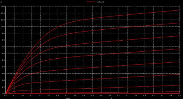
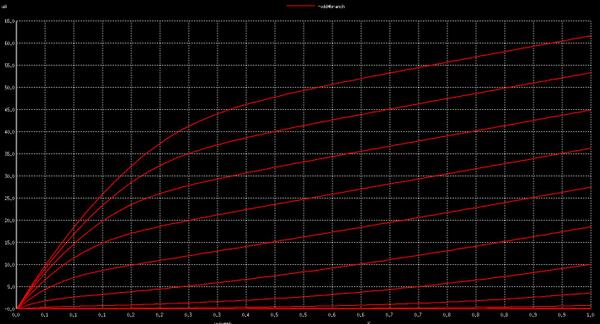
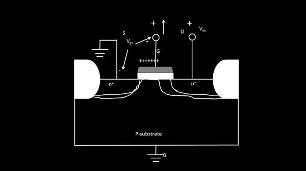
This is tricky. As Vds increases, the reverse bias near the drain region also increases. Due to shorter channel length of 32nm, the reverse bias touches source region. Boom….. that’s when source/drain merge into a single depletion region and drain current is no longer controlled by gate. This causes a rapid
increase in drain-to-source current, and which is what you see in above 32nm Id-Vgs curves.
Now as an STA engineer, that’s not my problem. My biggest problem is how do I model these complex effects of scaling in my libraries. Standard NLDM libraries just don’t help here. There are structural changes that can be done to NMOS transistor to protect punch-through effect. These extra
currents has great impact on gate delays (in my next blog, I will talk about Miller effect, which again brings in extra capacitance, and hence extra currents), and modelling delays with currents are best solution to capture these effects
Find it interesting…. well….just look forward for my course on CCS timing, which will be filled with such cool and
interesting concepts, and I can bet, you will not blink an eye while viewing the videos
Just like the saying goes, by Benjamin Franklin “An investment in knowledge pays the best interest”, my job is to make your investment interesting….
Till them stay tuned, finish below 4 courses 100% (below $11 coupon links valid till tomorrow, i.e. 7th feb 11:59pm IST), and happy learning
Circuit design and SPICE simulations – Part 1:
Circuit design and SPICE simulations – Part 2:
Static timing analysis – Part
1:
Static timing analysis – Part
2:
FYI: you can also get all my other courses at $11 using
below links, which is, again, valid till tomorrow, i.e. 7th feb 11:59pm IST
Physical design flow:
Clock tree synthesis – Part 1:
Clock tree synthesis – Part 2:
Custom
Layout:
Signal
integrity:
VLSI - Essential concepts
and detailed interview guide: