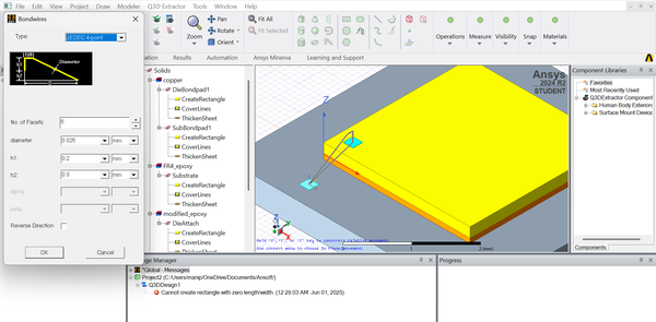
What you’re seeing:
- Yellow block → your silicon die
- Cyan rectangles → bondpads on die and substrate
- Black arc → a JEDEC 4-point bondwire with defined diameter, height, and shape
- FR4 layers → the PCB core and attach materials
The model extracts RLC parasitics from these geometries to help you understand:
- How inductive a 25µm wire becomes over 2mm span
- How loop height affects ringing
- How epoxy attach layers introduce impedance mismatch
This is where your design meets reality.
Why You Should Upskill Now
Engineers who understand packaging + sign-off + system behavior
are rare.
Those who can model both the inside of the chip and the world around it?
They're invincible.
And the best part? You don’t need expensive licenses or labs to start. You just need the right guided exposure.
Enroll Before It Closes – 1 Day Left!
To help you get there, we’re running a hands-on VLSI Packaging
Workshop – taught using real tools, real physics, and real case studies.
- Simulate bondwires, bumps, dies, PCBs
- Extract parasitics and visualize field behavior
- Co-simulate with actual circuit blocks
- Learn what 99% of STA engineers never touch
Register now – closes in 1 day: https://www.vlsisystemdesign.com/packaging/
Stop being a cog. Become a system designer.
When you master packaging, you stop just “closing timing” — and start designing systems that work, scale, and lead.
Make that leap.
See you inside the workshop.