Hi
Imagine this:
You’re days away from a critical chip tapeout when a setup timing violation emerges. The Slack is negative. The clock network is riddled with skew, and your team is scrambling. How do you fix this without delaying the project?
Welcome to the high-stakes world of Static Timing Analysis (STA) - a non-negotiable pillar of VLSI Physical design. Let’s break down how STA concepts like setup time, clock skew, and slack can make or break your design.
The Setup Timing Challenge (as covered in the
Digital SoC design program)
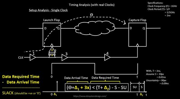
In synchronous circuits, data launched by a flip-flop must stabilize at the capture flip-flop before the next clock edge. The margin for this is defined by the setup time (S). Fail this, and your chip malfunctions.
Key Parameters:
- Clock Period (T): Time between two clock edges (e.g., 1 ns = 1 GHz).
- Data Arrival Time: Total delay
from launch clock edge to data reaching the capture flip-flop.
Data Arrival = Θ (launch clock delay) + Δ₁ (CLK-to-Q delay) + Combinational Delay (3x)
- Data Required Time: Latest time data can arrive without violating setup constraints.
Data Required =
T (period) + Δ₂ (capture clock delay) - S (setup time) - SU (uncertainty)
Slack = Data Required Time - Data Arrival Time
Slack ≥ 0? Your design passes. Slack < 0? Red alert.
The Tapeout Nightmare Scenario
Suppose your report shows:
- Θ = 0.2 ns (launch clock delay), Δ₁ = Δ₂ = 0.1 ns, Combinational Delay = 0.3
ns
- T = 1 ns, S = 0.01 ns, SU = 0.09 ns
Plugging into the equation:
Slack = (1 + 0.1 - 0.01 - 0.09) - (0.2 + 0.1 + 0.3)
Slack = (1.0) - (0.6) = **+0.4 ns** (Safe!)
Now, introduce a problem:
Due to routing congestion, the launch clock delay (Θ) increases by 0.3 ns (matching the combinational delay).
New Slack = 1.0 - (0.5 + 0.1 + 0.3) = **+0.1 ns**
Still safe, but margin is eroding. Now, add process variation increasing
combinational delay to 0.4 ns:
Slack = 1.0 - (0.5 + 0.1 + 0.4) = **0.0 ns** (Razor-thin margin).
One more delay spike, and Slack turns negative. Your tapeout is at risk.
Fixing the Crisis: STA in Action
- Clock Tree Tuning:
Balance clock
delays (Θ and Δ₂) to minimize skew. Use useful skew intentionally to shift capture clock timing. - Logic Optimization:
Break down long combinational paths (e.g., replace a 3x delay chain with pipelined registers). - Uncertainty Guardrails:
Revisit margin assumptions (SU). Is the 90ps uncertainty overly pessimistic? Validate with silicon data. - Advanced Techniques:
- Multi-Corner Multi-Mode
(MCMM) Analysis: Verify timing across PVT variations.
- Clock Domain Crossing (CDC) Checks: Ensure no metastability in asynchronous interfaces.
Why STA is the Backbone of VLSI
- Prevents Silicon Failure: A single setup violation can corrupt data across millions of transistors.
- Enables High-Frequency Designs: Tight Slack margins allow pushing clock speeds without
sacrificing reliability.
- Tool-Driven Precision: Industry tools like PrimeTime automate STA but require expert interpretation.
Final Takeaway
STA isn’t just a checkbox - it’s the difference between a functional chip and a costly respin. When the clock is ticking toward tapeout, mastering these concepts lets you diagnose violations, optimize paths, and ship with confidence.
Hungry for deeper insights? Explore hands-on strategies in our Digital VLSI SoC Design Workshop - where theory meets industry-grade execution.
Because in VLSI, timing isn’t everything…
it’s the only thing.