Hi
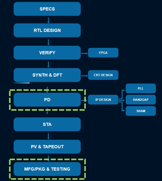
They say “a single image speaks a thousand words,” and the attached semiconductor design flow diagram exemplifies this perfectly. It captures the intricate journey from concept to silicon, highlighting critical stages like Physical Design (PD) and Manufacturing/Packaging &
Testing (MFG/PKG & Testing). Here’s how these phases anchor the value chain:
Physical Design (PD): The Backbone of Implementation
PD bridges the gap between logical design (RTL) and a manufacturable layout. It involves floorplanning, placement, routing, and clock tree synthesis to ensure timing, power, and area goals are met. At advanced nodes (e.g., 5nm), PD’s role becomes even more critical due to complexities like signal
integrity and thermal management.
Deepen your PD expertise: The course Digital VLSI SoC Design and Planning (registration closes in 2 days) offers hands-on insights into floorplanning, CTS, and sign-off checks.
Packaging & Testing: The Final Frontier
Post-fabrication, packaging transforms bare dies into functional chips while ensuring thermal stability and electrical connectivity. Testing (wafer/probe, final test) guarantees reliability, leveraging DFT structures to weed out defects. Advanced packaging (e.g., 3D ICs) is now pivotal for performance-driven applications.
Master modern packaging: Enroll in Advanced Semiconductor Packaging (registration closes in 4 days) to explore materials, thermal analysis, and cutting-edge techniques.
Why This Matters
The image simplifies the semiconductor value chain,
but PD and Packaging are where theory meets reality. PD ensures the design is manufacturable, while Packaging ensures it is market-ready. Both stages directly impact cost, performance, and time-to-market.
Act now to secure your spot in these courses and stay ahead in this fast-evolving field. Let’s discuss how these skills can elevate our projects!