Become an Industry‑Ready VLSI Designer (16 Hours Left!)
In 16 hours, registration for India’s premier full-stack VLSI design programs closes – act now to secure your spot.
India’s semiconductor industry is booming – projected to grow from a $38 billion market in 2024 to $105 billion by 2030. The
government’s ₹76,000 crore (≈ $10 billion) push for semiconductors is transforming India into a global chip design and manufacturing hub. What does this mean for you? An unprecedented demand for skilled chip designers and EDA experts. From Intel, Qualcomm, and NVIDIA to a wave of homegrown startups, companies are on a hiring spree for VLSI talent. By 2027, India will need hundreds of thousands of semiconductor professionals – now is your time to shine.
Why VSD-HDP
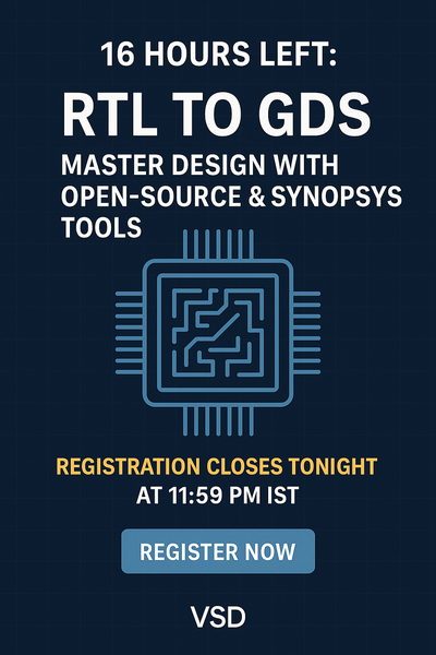
& VSD-SFAL? – Full-Stack RTL-to-GDS Training
To ride this semiconductor wave, classroom theory isn’t enough – you need cutting-edge, hands-on design experience. Our two flagship programs, VSD-HDP and VSD-SFAL, offer an immersive RTL-to-GDSII curriculum that bridges the gap between academic learning and industry requirements. You won’t be doing textbook labs; you’ll be tackling real chip
design challenges – from RTL coding and verification to floorplanning, power planning, placement & routing, clock tree synthesis, and timing sign-off on actual silicon technology.
Learn by Doing: These aren’t just exercises – they’re real-world projects that solve industry problems, making your training both practical and impactful. By working on real chip tape-out scenarios, you gain
specialized skills that make your résumé stand out to top employers.
Two Tracks, One Goal – Your VLSI Career Success: Whether you’re a final-year engineering student eyeing your first semiconductor job, a working professional looking to pivot into a high-growth chip design role, or a startup founder aiming to build your own silicon product, choose the training path that suits you:
- VSD-HDP (Hardware Design Program, Open-Source Track): Master the full digital design flow using open-source EDA tools. Plan and implement an SoC using the revolutionary Google–SkyWater 130nm open-source process (Sky130) within the OpenLANE flow – no expensive licenses needed. You’ll go from
RTL to GDS using tools like OpenLANE, Magic, and more, gaining a holistic understanding of how chips are built in an open-source ASIC workflow. (Ideal for learning fundamentals and building a strong foundation with accessible tools.)
- VSD-SFAL (Semiconductor Fabless Accelerator Lab, Synopsys Track): Train with
industry-standard Synopsys EDA tools used at top semiconductor companies. In this 12-week SoC design & implementation course, you’ll follow a professional RTL-to-GDS flow: synthesis with Design Compiler, block/APR with IC Compiler II, static timing analysis with PrimeTime, and more. You even get to implement a RISC-V based SoC on a 180nm foundry PDK – mirroring the real Synopsys-driven workflow used in fabless companies. (Ideal for experienced learners
who want to directly work with the tools and methodologies of the semiconductor industry.)
Industry Certification & Career Relevance: Upon completion, you earn a prestigious certificate to validate your expertise – a credential recognized by industry recruiters and sure to give your LinkedIn profile a boost. With India’s “Chips to Startup” initiative training 85,000+ chip engineers in coming years, you’ll
want every edge to stay ahead. These programs give you that edge by aligning with current hiring trends – from physical design engineer openings to growing demand in ASIC verification and EDA tool specialization. You’ll be job-ready for roles that are hot in the Indian semiconductor job market right now.
Urgent: Registration Closes Tonight at 11:59 PM IST
This is the
final call – less than 16 hours remain to secure your seat in the upcoming cohort. Don’t miss out on joining the semiconductor design revolution that’s sweeping India. Equip yourself with skills that put you at the forefront of technology, where innovation meets opportunity. Remember, the window shuts at 11:59 PM IST tonight – after that, you’ll have to wait and risk lagging behind your peers.
Ready to Launch Your VLSI Career? One decision now can fast-track your growth for the next 10 years. Seize this moment and invest in a career that’s driving the future of tech in India and beyond.
Register Now for VSD-HDP (Open-Source Track) - https://www.vlsisystemdesign.com/hdp/
Register Now for VSD-SFAL (Synopsys Track) - https://www.vlsisystemdesign.com/sfal/
See
you on the inside – let’s design the future together!
※ VSD-HDP and VSD-SFAL are brought to you by VLSI System Design (VSD), with a mission to empower India’s semiconductor talent. Enroll now to gain mentorship from experts, hands-on project experience, and an insider’s view into chip design workflows.