Hi
Registration for the Semiconductor Packaging: Design, Simulation, and Testing course closes in 13 hours
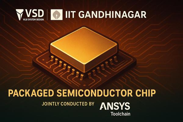
Enrol Now- https://www.vlsisystemdesign.com/packaging/
Why this matters for your career:
Semiconductor packaging is no longer a niche skill. With 3D integration, advanced thermal management (ANSYS labs), and reliability testing driving innovations in AI, EVs, and 5G, engineers who master packaging will lead India’s $100B+ semiconductor mission. This course dives deep
into:
- 3D/2.5D Packaging: Optimize die stacking for RISC-V and high-performance compute.
- Flip-Chip vs. Wire Bond: Choose the right assembly for RF/wireless or cost-sensitive designs.
- Thermal Simulation: Prevent overheating in data center/edge AI chips.
- Reliability Validation: Ensure packages survive automotive/industrial environments.
Act now - here’s what you’ll miss otherwise:
- Hands-on labs with ANSYS for thermal/mechanical modeling.
- Insights from industry veterans on selecting packaging architectures.
- A GitHub repository of past projects (link) to accelerate your learning.
50+ engineers have already enrolled. With companies like Intel, TSMC, and Indian startups aggressively hiring packaging experts, this is your chance to stand out.
Deadline: 24th April, 11:59pm IST
Secure your seat: https://www.vlsisystemdesign.com/packaging/
Don’t let this slip - your next career leap starts here.