Hi
You've mastered the challenges of physical design and tapeout. You can navigate congestion, manage timing closure, and deliver a clean GDSII. But what happens after the tapeout is often a "black box."
For a high-performance, power-efficient, and reliable
chip, the journey doesn't end at the GDSII. It enters the critical phase of Semiconductor Packaging.
If you think packaging is just about putting a plastic case around the die, you're missing a massive opportunity to elevate your design skills and your career
value.
Why Should a Physical Design or Floorplan Engineer Care About Packaging?
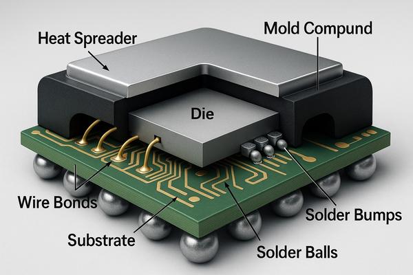
- System-Level Floorplanning: Your chip doesn't exist in a vacuum. The package substrate is its first PCB. Choices like Flip-Chip vs. Wire-Bond directly impact your die's I/O ring design, bump placement, and power distribution network (PDN). A poor floorplan can make a package impossible or prohibitively
expensive.
- Signal & Power Integrity (SI/PI): The package introduces RLC elements that affect signal quality and power delivery. Understanding this is crucial for high-speed interfaces (like DDR, PCIe, SerDes). Without this knowledge, your perfectly timed design can fail in the packaged system.
- Thermal Management: The primary path for heat dissipation is through the package. Your power map and hotspot locations must be communicated and aligned
with the package design to prevent thermal throttling or failure.
- Cost & Yield: The package often costs more than the silicon die. Your design decisions (die size, I/O count, bump pitch) directly dictate the package technology required, which is a huge driver of overall product cost.
Become the Irreplaceable, Full-Stack VLSI Engineer
The industry craves engineers who see the bigger
picture. By understanding the entire flow from RTL to final packaged product, you become the strategic linchpin on any team. You don't just design a die; you design a viable product.
You transition from a task-based engineer to a system-level architect, making you indispensable.
Master This Critical Knowledge in Our Intensive Workshop
We are closing registration for our exclusive workshop "Chip Packaging: The Bridge Between Silicon and System" TOMORROW.
This workshop is specifically designed for engineers like you who know physical design and want to complete the picture.
What You Will Learn:
- The complete packaging flow
after GDSII tapeout: from wafer test and dicing to die attach, wire bonding/Flip-Chip, and molding.
- How your floorplan and I/O planning decisions ripple through the packaging process.
- Overview of advanced packaging (2.5D/3D IC, CoWoS, InFO) that is defining the future of Moore's Law.
- The key trade-offs between performance, cost, thermal, and reliability.
This is your final call.
Registration closes in 1-day.
Don't let your expertise stop at the fab door. Add the final, critical piece to your skill set and become the truly holistic engineer that top companies are searching for.
Secure Your Spot Now: www.vlsisystemdesign.com/packaging/
Best regards,
The Team at VLSI System Design
P.S. This isn't a theoretical overview. It's a practical, deep dive into the interface between physical design and packaging. This knowledge is what separates good engineers from lead architects. Register before tomorrow's
deadline: www.vlsisystemdesign.com/packaging/