Hi
You know the story: process nodes keep shrinking. But at 7nm, the old rulebook was thrown out.
The challenges aren't just smaller transistors; they are entirely new physics and complex trade-offs that redefine how we design chips. If you're asked about
7nm in an interview, reciting a textbook definition won't cut it. They want to see you understand the implications.
This blog breaks down the three core paradoxes of 7nm and invites you to learn how to navigate them in our upcoming workshop. Registration closes in 1 day.
The 3 Paradoxes of 7nm Design
1. The Performance-Power
Paradox.
We scaled to 7nm for more speed and lower power, right? Yet, ultra-low threshold voltages lead to shocking leakage. Dennard scaling is over. You can't just plug in a 7nm library and get a win. The real skill is now in aggressive power management—using techniques like multi-Vt optimization, power gating, and clock gating together—to actually achieve those power savings. This is the first thing design teams have to solve.
2. The Complexity-Abstraction Paradox.
7nm processes use FinFETs (and now GAA). Their 3D nature makes them harder to model. On top of that, effects like layout-dependent stress and proximity effects mean the context of a transistor changes its behavior. The paradox is that while physics have gotten massively more complex, designers need higher abstraction (like RTL) to be productive. This is why
understanding the device-to-circuit interaction is no longer a nice-to-have; it's a core skill for every VLSI engineer.
3. The Cost-Access Paradox.
A 7nm mask set costs millions. This means only high-volume products can justify it, and there is zero room for error. Yet, open-source PDKs like the GF 7nm Learning Program are making this technology accessible for learning and research. The question is: will you be
among the first to get hands-on experience with it?
The Interview Angle: Why 7nm Questions Are a Trap
Interviewers don't ask "What is 7nm?" to hear a number. They ask it to see if you can articulate the shift in design mentality it requires.
- "What's the biggest difference between designing at 28nm and 7nm?"
- "How do FinFETs change standard cell design and
characterization?"
- "What are the biggest challenges to timing closure and power integrity at 7nm?"
- "How does variability affect design at advanced nodes?"
If you can move beyond the buzzwords and discuss the real engineering trade-offs, you demonstrate the deep understanding that gets job offers.
Learn it the right way: Hands-on with the 7nm PDK
Workshop: Physical Design and Timing Analysis using 7nm Technology
Register: www.vlsisystemdesign.com/7nm/
Deadline: Closes in 1 day
What You’ll Do: Master Circuit Design at the 7nm Node
This workshop is a deep dive into
the practical reality of designing circuits with 7nm FinFETs. You will move from theory to simulation, characterizing devices and building fundamental circuits with the industry-standard ASAP7 PDK.
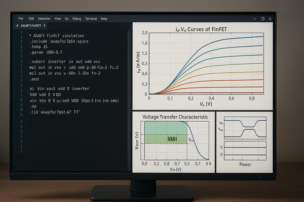
- Setup the 7nm Environment: Install the ASAP7 PDK and configure your Xschem/NGspice workflow, running your first simulations to validate the setup.
- Characterize 7nm FinFETs: Extract and analyze NFET/PFET I-V curves to understand
drive current, transconductance (gm), and output resistance (ro), choosing optimal bias points for design.
- Design a 7nm Inverter: Build a fundamental CMOS inverter, accounting for fin quantization, and script the simulation to plot its Voltage Transfer Characteristic (VTC).
- Measure Performance & Robustness: Quantify key metrics: noise margins (NML/NMH), propagation delay, dynamic
power, and static leakage current across various loads and input slews.
- Perform PVT Sign-Off Analysis: Run simulations across process corners (TT, FF, SS), voltage variations (±10%), and temperatures (-40°C to 125°C). Learn to set pass/fail criteria and summarize performance for a robust design.
- Design a Bandgap Reference Circuit: Implement and analyze a self-cascode MOS bandgap reference, a critical analog block, and
characterize its performance at the 7nm node.
- Analyze Stability & Regulation: Test your circuits for real-world conditions, sweeping line and load to measure line regulation, load regulation, stability, and startup behavior.
Who should join
- Aspiring physical design, CAD, and timing engineers.
- RTL designers and verification engineers who need to understand the physical implications of their code.
- Students and
professionals aiming for roles at companies working on cutting-edge CPUs, GPUs, and AI accelerators.
What you’ll take away
- The ability to speak confidently about 7nm not as a magic number, but as a set of solvable engineering challenges.
- Hands-on experience with the industry's most advanced publicly available PDK.
- A foundational understanding of the entire physical design flow for advanced nodes.
A 30-second interview script you can
practice
Q: What are the key differences when designing at 7nm compared to older nodes?
A: *It's a shift from pure performance optimization to managing complex trade-offs. The three biggest changes are: 1) Power management becomes paramount due to leakage, requiring advanced techniques like multi-Vt optimization. 2) Physical effects like layout-dependent stress and variability have a first-order impact on timing and power,
making accurate modeling essential. 3) The immense cost of tapeout demands a zero-error flow, elevating the importance of signoff-quality verification throughout the design process.*
Seats are limited and registration closes in 1 day.
If you want to move from theoretical node names to practical, hands-on skills that are in high demand, this is your chance.
Join the workshop now: www.vlsisystemdesign.com/7nm/