Hi ,
Every digital chip—no matter how “system” the job title sounds—still rises and falls on one primitive: the MOSFET. The difference between engineers who just “run the flow” and those who consistently close designs is device-level intuition. That’s why we built CMOS Circuit Design & SPICE Simulation
using SKY130: a hands-on path to mastering the physics that drives timing, power, signal integrity and reliability across an ASIC.
Enroll: https://www.vlsisystemdesign.com/cmos-circuit-design-spice-simulation-using-sky130-technology/
Why CMOS/MOSFET fundamentals change outcomes (evidence from the flow)
- Process/PDK choices → better corner thinking: Understanding VTV_TVT, body effect, DIBL and mobility lets you read BSIM models, select LVT/SVT/HVT devices, and predict delay/leakage shifts before synthesis.
- Standard-cell behavior → correct fixes: gmg_mgm, ror_oro, and gate/junction caps map directly to cell drive, slew and logical effort—so you know whether to upsize, buffer, or
V_T-swap on a failing path.
- Library characterization → what .lib really means: On-current and capacitances become delay/power tables. You can interpret liberty views and guide multi-V_T leakage recovery with confidence.
- Timing closure (STA) → fewer ECO loops: Short-channel effects and parasitics explain AOCV/POCV derates and waveshape; you pick the right fix for setup/hold instead of
trial-and-error.
- Low-power design → real savings, not slides: Stacking effect, subthreshold and gate leakage, body-bias and power gating translate into measurable standby power wins.
- Signal integrity/clocking → stable silicon: Miller coupling and non-linear CCC tell you when to shield, space, or slow edges—reducing late-stage crosstalk and
jitter surprises.
- Physical design/DFM → cleaner sign-off: Antenna risk (thin gate oxide), latch-up, EM limits and multi-finger devices lead to fewer DRC/LVS/IR-drop violations.
- Extraction & post-layout → correlation that holds: Knowing where fringe and diffusion caps come from explains pre vs. post timing shifts and avoids over- or under-design.
- Reliability & ESD → yield that
lasts: BTI/HCI/TDDB and clamp device choices protect performance over life; you set credible aging derates and pass qualification.
What you’ll practice in this course
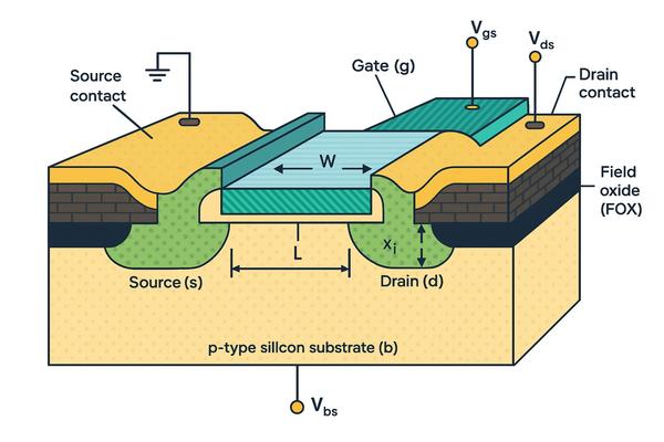
- Work with the open-source SKY130 PDK and SPICE to sweep I–V curves, extract VTV_TVT, gmg_mgm, ror_oro and key capacitances.
- Build and simulate CMOS logic (inverter →
NAND/NOR, pass-gate, level shifter); analyze noise margins, delay vs. load/voltage, and dynamic vs. leakage power.
- Run corner simulations to see variability; relate device effects to timing/power the same way sign-off tools do.
- Connect device-level results to library behavior you see in .lib and to STA fixes you apply in practice.
Who benefits
Physical design & STA • Library/Memory & analog • IO/ESD & reliability • DFT/validation • EDA modeling • Senior students aiming for front-/back-end roles. If your job touches timing, power, SI, or reliability, deep CMOS intuition pays back immediately.
Career outcomes you can claim
- Translate device parameters to cell selection and optimization (LVT/HVT/size) for timing/leakage
closure.
- Diagnose failures as device-driven (cap/leak/ro) vs. interconnect-driven (RC/crosstalk)—cutting ECO cycles.
- Produce SPICE-backed plots (delay vs. VDD, leakage vs. V_T, slew vs. Cload) that strengthen design reviews and interviews.
If you want a sustainable edge in VLSI—whether you’re closing clocks, building libraries, or signing off reliability—start where the physics
meets the flow.
Enroll today: https://www.vlsisystemdesign.com/cmos-circuit-design-spice-simulation-using-sky130-technology/
Best regards,
Kunal Ghosh, Founder
VLSI System
Design (VSD)
P.S. Teams enrolling together can align the course labs with their current block or library work; reply if you’d like a cohort plan for your project.