Hi
Why 7nm? Because it’s the workhorse node behind today’s flagship SoCs, AI accelerators, 5G basebands, high-speed SerDes/PHYs, and automotive ADAS compute. FinFETs at 7nm deliver the PPA sweet spot industry still tapes out on - so teams hire engineers who can think at the device ↔ circuit boundary
and sign off with data.
Introducing FinFET Circuit Design and Characterization (7nm) — a hands-on workshop that turns advanced-node theory into a verifiable portfolio.
What you’ll build (and show):
- NFET/PFET at 7nm: Id–Vd/Id–Vg, gm, ro, practical bias points
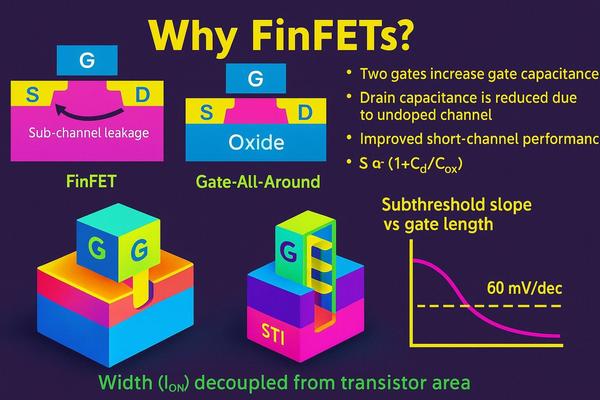
- Inverter VTC & noise
margins: sizing with fin quantization, delay/power vs load
- Precision bandgap (Self-Cascode MOS): VREF vs temperature, line/load regulation, startup
- Deterministic PVT: scripted .measure flows, clean plots, and a check-listed sign-off pack
Why this program stands out:
- Carefully designed assignments with checkpoints, reference
decks, and plotting templates
- Three years of R&D - evolved from our 7nm contest (2022) into a tight, industry-aligned curriculum
- Open, reproducible toolchain: ASAP7, Xschem, Ngspice - skills that transfer to Spectre/HSPICE flows
Who should join:
- UG/PG/PhD students aiming for semiconductor internships or research
- Working engineers
(analog/ASIC, mixed-signal, verification) upskilling to advanced nodes
- Faculty/startups building credible nanoelectronics labs
Outcomes:
A reviewable GitHub repo (netlists, scripts, plots), a validated 7nm workflow, and a VSD certificate - evidence recruiters and product teams trust.
Details & registration: https://www.vlsisystemdesign.com/7nm/
If you’re serious about the future of VLSI computing - and your role in it - this is your start.