Hi
Registration for our intensive Semiconductor Packaging Workshop closes in 12 hours. This is your last chance to gain hands-on skills in cutting-edge packaging technologies used by Top Semiconductor companies.
Core Technical
Curriculum
- Advanced Packaging Architectures
- Design/analyze 2.5D CoWoS, flip-chip BGA, and chiplet-based systems (Section 1.D)
- Material selection tradeoffs: organic laminates vs. silicon interposers (Tables 1.C.1, 1.D.1)
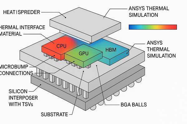
- ANSYS Electronics Desktop Labs
- Thermal simulation of FC-BGA packages (Module 3)
- Parametric analysis of solder bumps, underfill, and mold compounds (Section
3.D)
- OSAT/Foundry Workflows
- Wafer dicing → die attach → wire bonding → molding (Section 2.C)
- Burn-in testing and corner validation (LM741C case study, 4.B.2)
- Reliability Engineering
- Detect head-on-pillow defects, electromigration via AOST (Section 4.A.3)
- Thermal cycling + SLT methodologies (Figures 4.1, 4.2)
Hardware/Tools
Proficiency
- ANSYS Icepak/Q3D: Model thermal distribution in multi-die stacks (Section 5)
- ATE Handlers: Execute hot/cold testing (-40°C to 125°C)
- Industry datasets: Micron ATMP plant layouts, NVIDIA H100 interposer specs
Outcomes
- Build portfolio-ready package models (e.g., wire-bonded QFN, flip-chip PBGA)
- Certificate: Advanced Package Reliability
Engineer
- Access to VSD’s BGA design rule-checks (DRC) kit
Act Now
- Registration Deadline: 12 hours from now
- Limited seats: 40 participants max for lab access
- Enroll Here: https://www.vlsisystemdesign.com/packaging/
Why Attend?
*“Section 3’s ANSYS FC-BGA
thermal simulation alone helped me optimize heat dissipation in our data center GPUs.”*
— Senior Engineer,
This workshop bridges theory (e.g., substrate I/O routing) and practice (e.g., underfill dispensing DOE). Miss this, and you miss industry-relevant skills in the $65B OSAT market.
Finalize Enrollment: https://www.vlsisystemdesign.com/packaging/
Best regards,
Kunal Ghosh
VLSI System Design (VSD) Team