Hi
When timing breaks after a late VDD change, the root cause is rarely “mystery.” It’s device physics: Vm shifts with sizing, gain collapses near low‑VDD, and noise margins tighten under corners. Teams that measure these effects - rather than assume textbook curves - close timing faster and cut ECO
churn.
This cohort is designed to produce that proof.
What you will actually build in 10 days (and why it matters):
- VTC dossier with sizing laws: You will generate Vout‑vs‑Vin curves while sweeping (Wp/Wn) and extract Vm and dVout/dVin at Vm. Outcome: a sizing rule of thumb for balanced tPLH/tPHL that maps directly
to library choices in PD and STA.
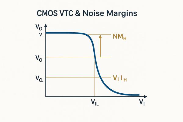
- Noise‑margin ledger under PVT: You will compute NMH/NML at TT/SS/FF and show how margins move with load and sizing. Outcome: defensible input‑level assumptions for STA thresholds and glitch‑tolerance discussions.
- Supply‑scaling trade‑off report: You will sweep VDD from 1.8 V toward sub‑1 V, quantifying gain around Vm and the corresponding delay/energy impact. Outcome: a concrete
argument for low‑power modes that doesn’t guess.
- Inverter‑chain timing sanity test: You will measure delay vs load across a short chain to see how channel‑length modulation and sizing interact. Outcome: intuition you can reuse when evaluating ECO buffers.
Why this cohort is different:
- Falsifiable targets: Each lab has acceptance criteria (e.g., “|dVout/dVin| at
Vm ≥ target at TT,” “ΔVm vs 2×PMOS width within range”). You leave with numbers, not vibes.
- One deck, many answers: Parameterized NGSpice decks (SKY130 PDK) drive all sweeps; you change values, not tools.
- Direct line to production reality: Every plot is tied to a PD/STA/ECO decision you make later—thresholds, derates, buffer choices, low‑VDD feasibility.
- Cloud simplicity, real mentorship: Zero local installs; launch the
VDI on day one. Mentors cover time zones with near‑continuous support.
If you’ve wanted a concise, defensible way to connect transistor‑level behavior to backend outcomes, this is it. Registration closes tonight at 11:59 PM IST. As a last‑day bonus, enroll today and you’ll receive a private 20‑minute 1:1 lab review during the program to tune your decks and interpretation.
Details and enrollment:
https://www.vlsisystemdesign.com/cmos-circuit-design-spice-simulation-using-sky130-technology/
Regards,
VLSI System Design (VSD) Teaching Team
PS If you are certain your CMOS fundamentals already withstand rigorous production scrutiny, please feel free to pass this along to a colleague who would benefit.