Dear VLSI enthusiast,
After mentoring 1,000 + learners over the past five years—ranging from first‑year undergrads to seasoned timing‑closure engineers—one pattern has become crystal clear:
The MOSFET intuition we pick up in textbooks
rarely survives first contact with real‑world silicon.
Threshold voltage that drifts with body bias, velocity saturation that flattens your carefully plotted curves, noise margins that crumble under lower supply rails—these behaviours often feel like footnotes in a lecture but loom large in production tape‑outs.
That is why we invite you to take a brief, liberating
step:
1. Un‑learn the “ideal” MOSFET
Forget, for a moment, the perfectly linear resistive region or the saturation current that never budges. Set aside the hand‑drawn square‑law curves that live only on whiteboards. Industry silicon does not read our favourite chapters; it follows physics, process corners, and PVT quirks.
2. Re‑learn CMOS the industry way
The
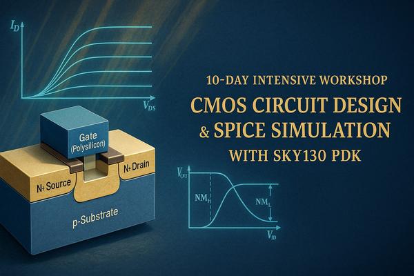
most efficient path we’ve discovered is an open‑source one—SKY130, the mature 130 nm process now powering university shuttles, start‑ups, and corporate prototyping alike. By building and breaking circuits in the SKY130 PDK with NGSpice, you will see every assumption challenged in live plots:
- Id‑Vds sweeps that reveal channel‑length modulation in action
- VTC curves shifting as you resize PMOS/NMOS pairs for balanced
delays
- Noise‑margin tests that uncover how real inverters shrug—or shatter—under glitches
- Supply‑scaling labs that trade gain for energy, just like today’s IoT chips
3. Apply the new mindset to PD, STA, and ECO
Backend domains thrive on accurate device awareness. Whether you debug hold violations, craft ECO libraries, or sign off IR‑drop, re‑calibrated
MOSFET instincts shorten iterations and reduce late‑stage surprises. Alumni of our program routinely report faster timing convergence and more confident corner analysis after re‑grounding themselves in transistor‑level reality.
The Workshop That Makes Un‑learning Enjoyable
Our ten‑day, cloud‑hosted course—“CMOS Circuit Design & SPICE Simulation using SKY130 Technology”—was built precisely to guide this
transformation:
- Daily mini‑projects turn concepts into plots you can see and measure
- Round‑the‑clock mentor support (via WhatsApp) keeps every timezone in sync
- No local installs—a ready VDI workspace launches your first NGSpice deck in minutes
- Capstone inverter chain proves you can size for speed and noise immunity under TT/SS/FF corners
Most important of all, the atmosphere is deliberately humble and peer‑driven. We remember what it felt like to redraw square‑law curves for the hundredth time - only to watch silicon misbehave. So every lab starts with a clean slate, inviting you to question why before memorising how.
Explore the syllabus and enrol:
https://www.vlsisystemdesign.com/cmos-circuit-design-spice-simulation-using-sky130-technology/
A Gentle Call to Action
If you aspire to excel in Physical Design, Static Timing Analysis, ECO, or any path that leans on robust CMOS insight, we warmly encourage you to join the growing community that has chosen to
un‑learn first - and emerge stronger.
We are here to support, clarify, and celebrate each “aha!” moment with you.
Looking forward to un‑learning together,
The VSD Teaching Team
VLSI System Design (VSD)
“Learn. Un‑learn. Re‑learn. Design.”