Hi
The semiconductor industry is evolving fast. While Physical Design and STA remain core skills, Semiconductor Packaging is where real-world challenges begin.
Industry reports project that by 2030, over 30% of chip design jobs will
require packaging knowledge, driven by advanced technologies like 2.5D/3D ICs, chiplets, and heterogeneous integration.
Packaging engineers are no longer assembly-line workers—they are system architects, working on:
- Signal integrity optimization
- Power delivery network (PDN) planning
- Thermal management of high-density dies
- 3D EM simulations of interconnect
parasitics
If you want to be part of this next-gen workforce, the time to start is now.
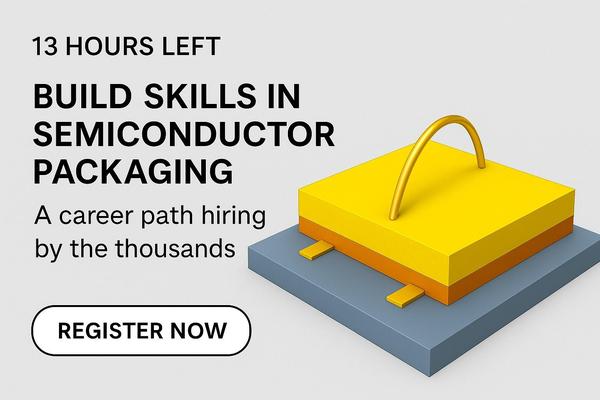
✅ Last 8 cohorts of our hands-on Semiconductor Packaging Workshop are open for registration—closing in 13 hours.
This workshop teaches you how to model real-world packaging elements like bondwires, die-attach, and substrate layers, using industry-grade
simulation flows.
You’ll gain skills that companies are actively hiring for, across design, testing, and manufacturing roles in the semiconductor domain.
👉 Register now before it closes:
https://www.vlsisystemdesign.com/packaging/
Prepare today for careers that will dominate the chip design landscape tomorrow.