Hi
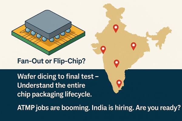
Physical design has pushed silicon to remarkable limits, but the next performance frontier now lies beyond the die. Advanced packaging techniques - fan-out, 2.5 D, 3 D ICs, chiplets - unlock bandwidth and efficiency gains that layout optimizations alone can no longer deliver. If you already understand timing
closure and floorplanning, mastering packaging lets you extend that expertise into the domain where every connection, bump, and thermal path directly shapes a product’s success.
Our fast-track Semiconductor Packaging Workshop distills these skills into a concise, application-driven program covering substrate design, signal- and power-integrity co-analysis, thermal management, and reliability testing. You will leave
with an end-to-end view of how today’s chips move from GDSII to fully-stacked systems—precisely the knowledge India’s emerging OSAT and ATMP facilities need right now.
Registration closes in 24 hours; secure your seat here:
https://www.vlsisystemdesign.com/packaging/
Thank you for your time, and I look forward to seeing you at the workshop.
Best regards,
Kunal Ghosh
Founder, VLSI System Design (VSD)