Hi
The semiconductor industry is at the heart of technological innovation, powering everything from smartphones to electric vehicles. While chip design and fabrication often steal the spotlight, semiconductor packaging—the art of protecting, powering, and connecting chips to the world—is rapidly
emerging as a critical frontier. India, with its growing pool of engineers and tech enthusiasts, is quietly building a talent pipeline to master this domain. With initiatives like the Packaging Fundamentals of Design and Testing repository and specialized courses such as VLSI System Design’s Semiconductor Packaging Program, the country is preparing engineers to bridge the gap between chip design and real-world applications.
Here’s why packaging expertise is becoming indispensable for semiconductor professionals - and how India’s upskilling efforts are creating a new generation of
innovators.
1. Packaging Evolution: From Basics to 3D Integration
Why It Matters for Engineers
Modern packaging isn’t just about enclosing a chip—it’s about enabling performance, power efficiency, and miniaturization. For physical design engineers and RISC-V developers, understanding packaging architectures is critical:
- 3D Integration: Stacking dies vertically
(e.g., HBM in GPUs) reduces latency and power consumption. RISC-V-based AI/ML chips leverage this for high-speed data transfer.
- Interposers & Redistribution Layers (RDLs): These enable heterogeneous integration, connecting logic, memory, and analog chips. Engineers designing IoT or edge devices must optimize these interconnects.
- Multi-Chip Modules (MCMs): Used in automotive electronics, MCMs combine diverse dies (sensors, processors) into a
single package.
Real-World Impact: Engineers who master packaging can design systems that are smaller, faster, and more reliable—key for India’s ambitions in EVs, 5G, and defense electronics.
2. From Wafer to Package: Assembly and Manufacturing Essentials
Connecting the Dots for Physical Design Engineers
The journey from wafer to package involves precision processes like
grinding, dicing, and flip-chip assembly. For engineers:
- Wafer Thinning: Impacts thermal performance—vital for high-power processors.
- Flip-Chip vs. Wire Bond: Flip-chip offers better electrical performance (critical for RF/wireless chips), while wire bonding remains cost-effective for legacy designs.
- Supply Chain Insights: Understanding facilities and material sourcing helps engineers optimize for yield and cost—a must
in India’s cost-sensitive market.
Takeaway: Engineers who grasp manufacturing nuances can avoid costly design re-spins and collaborate effectively with foundries.
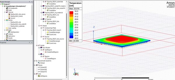
3. Labs: Thermal Simulation with ANSYS
Why Thermal Management is Everyone’s Problem
Overheating is the nemesis of performance. In the lab, engineers simulate heat dissipation in packages like Flip-Chip BGAs
using ANSYS. For RISC-V engineers building edge AI chips or physical design experts working on FPGAs:
- Power Density: High-performance chips (e.g., data center processors) require advanced cooling solutions.
- Material Selection: Mold compounds and underfill materials affect reliability in harsh environments (automotive, aerospace).
Practical Skill: Thermal
simulation expertise makes engineers indispensable in industries like consumer electronics, where thin devices demand efficient heat management.
4. Ensuring Reliability: Testing & Validation
The Bridge Between Design and Market Success
A chip that fails under stress can sink a product. For electronics engineers:
- Electrical Testing: Validating signal integrity in high-speed
interfaces (PCIe, DDR5) is crucial.
- Accelerated Life Testing: Simulating years of operation in days ensures packages survive India’s extreme climates.
Career Edge: Engineers who understand reliability can lead failure analysis teams—a high-demand role in automotive and industrial sectors.
5. Package Design & Modeling: Building from Scratch
From Concept to
Cross-Section
Using ANSYS, engineers model every layer of a package, from die attach to wire bonds. For RISC-V SoC designers:
- Signal Integrity: Modeling helps avoid crosstalk in dense interconnects.
- Mechanical Stress: Ensures packages withstand vibrations in automotive systems.
Innovation Playground: Custom package design enables startups to differentiate their IoT
or wearables with compact, high-performance solutions.
Why India’s Talent Pipeline is a Game-Changer
India’s tech ecosystem is buzzing with engineers hungry to master packaging. The GitHub repository showcases past participants’ work - proving that hands-on learning is
already underway. Now, the VLSI System Design Packaging Course is accelerating this momentum by offering:
- Industry-Aligned Curriculum: From 3D integration to ANSYS labs.
- Career Relevance: Packaging skills complement existing expertise in RTL design, PD, and verification.
- Global
Opportunities: With companies like Intel, AMD, and TSMC investing in advanced packaging, skilled engineers can work on cutting-edge projects worldwide.
Join the Packaging Revolution
Semiconductor packaging is no longer a “back-end” task—it’s where innovation meets reality. For engineers in India and beyond, mastering this field unlocks opportunities in AI, automotive, and beyond.
Ready to
explore?
The future of electronics is packaged - be the engineer who delivers it.