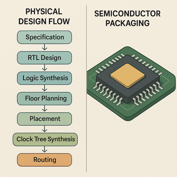
2. Workshop 2: Semiconductor Packaging – Thermal Analysis, Design, and Testing
Enroll Now
What You’ll Learn:
Packaging is where silicon meets the real world. This
workshop covers substrate design, thermal management, signal integrity, and advanced testing methodologies for packages like Flip-Chip Ball Grid Array (FC-BGA).
Hands-On Lab Highlight:
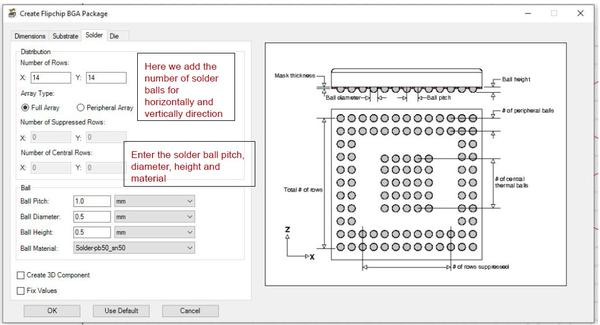
- Lab Image Spotlight: Thermal analysis of an FC-BGA package using Ansys AEDT. Learn to simulate heat dissipation and optimize package reliability.
- Create a Cross-Sectional View: Use Ansys to
model and analyze semiconductor package structures, ensuring robustness against mechanical and thermal stress.
Why It Matters:
As chips shrink and power densities rise, packaging innovation is key to preventing overheating and ensuring longevity. India’s packaging and testing market is expected to grow at 15% CAGR, driven by IoT, automotive, and defense sectors.
The Future of Jobs: Why Start
Now?
- Physical Design Careers:
- India: Entry-level salaries range from ₹6–12 LPA, soaring to ₹20+ LPA for roles like Physical Design Engineer or CAD Manager.
- US: Average salaries hit 100,000–100,000–180,000, with demand surging due to the CHIPS Act.
- Semiconductor Packaging Careers:
- India: Salaries start at ₹5–8 LPA, reaching ₹18 LPA+ for specialists in thermal or RF packaging.
- US: Roles like Packaging Engineer offer 90,000–90,000–160,000, driven by AI, automotive, and aerospace sectors.
- Industry Growth:
- India’s “Make in India” and $10 billion semiconductor incentive scheme aim to create 1 lakh jobs by 2030.
- The US plans to invest $52 billion in domestic chip manufacturing, needing 70,000+ skilled
engineers.
Nation Building Starts with You
By mastering these skills, you’re not just securing a lucrative career—you’re empowering India’s semiconductor independence. Skilled engineers reduce reliance on imports, drive R&D, and position India as a global innovation leader.
Act Now – Limited Seats!
- Workshop Dates: 9th April
- Lab Access: Use
cutting-edge tools like Ansys AEDT.
- Certification: Earn industry-recognized credentials to stand out in job markets.
Register for Digital VLSI SoC Physical Design
Register for Semiconductor Packaging
Be the Architect of Tomorrow
The semiconductor revolution is here. Whether you’re designing the next billion-transistor chip or ensuring its reliability in harsh environments, your expertise will shape industries and economies. Enroll today and build the future—one transistor, one package at a
time.
🚀 Lab images attached below showcase the hands-on, industry-aligned training awaiting you! 🚀