Hi
The journey from RTL (Register Transfer Level) to GDSII in modern System-on-Chip (SoC) design is a complex, multi-stage process that demands precision, expertise, and hands-on experience with industry-standard tools. For aspiring VLSI engineers, navigating this flow—synthesis, floorplanning, clock tree synthesis,
routing, and signoff—can seem daunting. However, structured programs like the Semiconducto Fabless Accelerator Labs (SFAL) bridge this gap, transforming theoretical knowledge into practical mastery. Over 12 weeks, participants gain proficiency in Synopsys EDA tools while tackling real-world projects, making the program a
catalyst for career growth in semiconductor design.
Decoding the SoC Design Flow: A Synopsys-Driven Approach
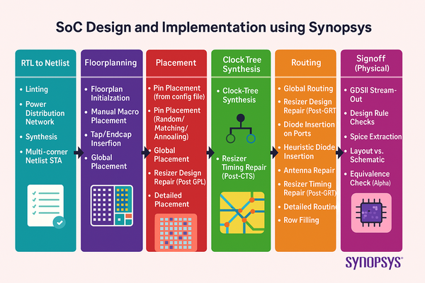
The SFAL curriculum mirrors the industry-standard SoC implementation flow, as illustrated in the design flow diagram. Here’s how the program translates each stage into actionable learning:
- RTL to Netlist: Building a Solid Foundation
- Linting, Synthesis, and STA: Participants learn to validate
RTL code using Synopsys VC Formal and synthesize it into gate-level netlists with Design Compiler. Multi-corner STA (Static Timing Analysis) using PrimeTime ensures timing closure across process variations.
- Power Distribution: Techniques for robust power grid design are emphasized, preparing learners for low-power challenges.
- Floorplanning: Crafting the Chip’s Blueprint
- Tools like IC Compiler guide trainees in floorplan initialization,
macro placement, and tap/endcap insertion. Manual macro placement exercises instill an understanding of area-performance tradeoffs.
- Placement: Precision and Optimization
- From global placement to detailed pin alignment, SFAL covers automated and heuristic methods. Post-placement optimization using tools like Innovus ensures design rule compliance and timing fixes.
- Clock Tree Synthesis: Timing at the Heart
- Clock
tree synthesis (CTS) workshops focus on minimizing skew and latency. Post-CTS timing repairs using PrimeTime reinforce the importance of a robust clock network.
- Routing: Connecting the Dots
- Trainees tackle global routing, antenna effect mitigation, and detailed routing using Synopsys tools. Real-world issues like diode insertion and design rule violations are resolved hands-on.
- Signoff: The Final Checkpoint
- GDSII
generation, DRC/LVS checks (using IC Validator), and equivalence verification ensure tapeout readiness. SPICE extraction and layout vs. schematic (LVS) comparisons cement the importance of accuracy.
The SFAL Advantage: Structured Learning for Real-World Impact
What truly sets SFAL apart is its product-oriented curriculum, meticulously designed to mirror industry workflows while fostering specialization and
professional growth. Here’s how the 12-week journey unfolds:
- Weeks 1–6: Mastering the Fundamentals
- The first phase immerses learners in semiconductor design essentials: floorplanning, placement, CTS, routing, optimization, and verification.
- Hands-on labs cover everything from chip size estimation to signal integrity fixes, ensuring participants grasp not just “how” but “why” each step
matters.
- Specialization Phase: Tailored Expertise
- After mastering the basics, students choose a specialization topic (e.g., low-power design, advanced timing closure, or physical verification).
- Guided by industry experts, this phase enables targeted skill development, aligning with individual career goals or emerging industry trends.
- Weeks 7–10: Industry-Grade Projects
- The program shifts to advanced concepts led
by professionals, focusing on challenges like multi-voltage designs, IR drop analysis, and congestion resolution.
- Participants work on a capstone project that mirrors real-world tapeouts, integrating Synopsys tools to solve problems faced by today’s design teams.
- Weeks 11–12: Professional Readiness
- The final phase prepares students for the workplace, covering GitHub documentation, collaborative workflows, and
internship/job selection strategies.
- Mock interviews and resume-building workshops ensure graduates stand out in a competitive job market.
Why SFAL Stands Out
- Industry-Aligned Projects: From day one, learners apply Synopsys tools to solve
problems like antenna violations, clock tree optimization, and DRC fixes—skills directly transferable to roles in top semiconductor firms.
- Expert Mentorship: Seasoned professionals share insights on tradeoffs, debugging, and best practices, bridging the gap between academia and industry.
- Specialization + Breadth: The blend of foundational training and focused specialization ensures graduates are versatile yet deeply skilled in high-demand
areas.
Transforming Careers: Freshers and Professionals Alike
For freshers, SFAL demystifies the EDA toolchain, turning academic concepts into tangible skills. One alum shared, “I’d never touched a place-and-route tool before SFAL. Now, I can confidently discuss floorplanning strategies in interviews.”
Professionals benefit equally. A
design engineer transitioning from analog to digital domains noted, “The program’s focus on signoff STA and multi-corner analysis filled critical gaps in my knowledge. The capstone project gave me a portfolio piece that impressed my current employer.”
Join the Next Cohort
The SFAL program isn’t just about learning tools—it’s about thinking like a designer. Whether you’re a recent graduate aiming to break into VLSI or
a professional seeking to upskill, the structured 12-week journey offers:
- Phased Learning: Build expertise step-by-step, from fundamentals to specialization.
- Real-World Impact: Tackle projects that replicate industry challenges, guided by Synopsys tools and mentors.
- Career Readiness: Graduate with polished documentation skills, a professional portfolio, and industry connections.
Ready
to transform your understanding of SoC design? Explore how SFAL can accelerate your career at https://www.vlsisystemdesign.com/sfal/.
The future of semiconductor innovation relies on skilled engineers. Equip yourself with the tools to lead it.