Hi
Physical design expertise is non-negotiable in today’s semiconductor industry. Yet, lab-intensive courses that simulate real-world PD workflows—especially at costs accessible to students and early-career engineers—are rare.
The NASSCOM Physical Design Program is an exception.
Why This Program is Unique
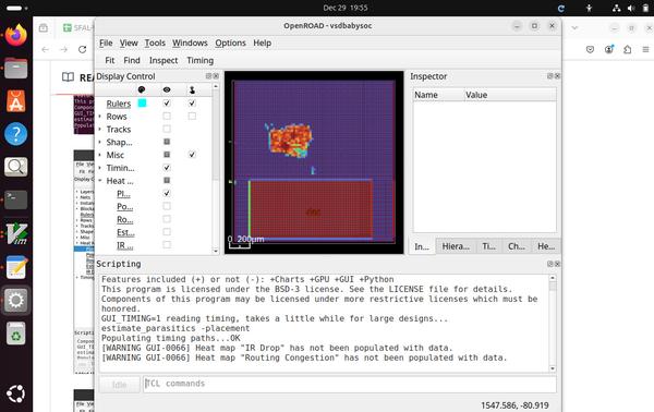
- Industry-Grade Labs: Work hands-on with open-source EDA tools (OpenROAD, Magic) to implement RTL-to-GDSII flows, mastering:
- PDK interpretation (layer
stacks, DRC rules, LVS decks).
- Floorplanning, power grid design, and clock tree synthesis.
- Signal integrity analysis and DRC closure in advanced nodes.
- Direct Commercial Tool Readiness: The principles learned apply seamlessly to Cadence/Synopsys environments.
- Unmatched Cost: At 1/10th the price of corporate trainings, this is the most affordable path to tapeout-ready skills.
Act Now – Registration Closes in 24 Hours
Seats are strictly limited to maintain mentorship quality. Payments must be completed before 11:59pm IST, 25th March, 2025 to secure access.
Enroll & Pay Here --> https://vsdsquadron.vlsisystemdesign.com/digital-vlsi-soc-design-and-planning/
Bottom Line
If you’re serious about leading in VLSI PD, this is your last chance to:
- Build a portfolio of DRC-clean designs.
- Transition from academic theory to industry practice.
- Compete for roles at top semiconductor firms.
Delaying risks losing this rare, low-cost,
high-impact upskilling opportunity.
Final Deadline: 25th March, 2025, 11:59 PM IST.
Best regards,
Team VSD
P.S. Preview the lab rigor via our GitHub repo. Do not wait—seats are forfeited after the deadline.