Hi
India’s semiconductor industry is poised for exponential growth, with the chip packaging market projected to reach $10 billion by 2030. Yet, a critical talent gap threatens this momentum. NASSCOM, Ansys, IIT Gandhinagar, and VSD worked aggressively for last 6-months, are
bridging this gap through a groundbreaking initiative designed to empower engineers with cutting-edge skills in chip packaging - starting with simulations, ending with industry-ready expertise. (Labs are available only for Windows OS Users)
Why This
Matters:
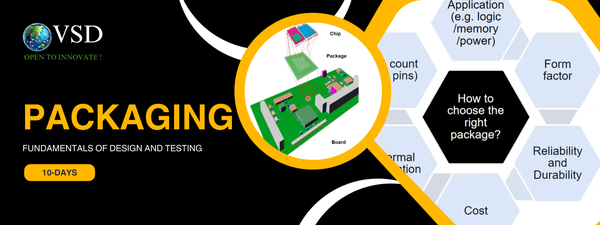
- Industry 4.0 Demands Expertise: Advanced packaging technologies like 3D ICs and heterogeneous integration are revolutionizing electronics.
- Learn from the Best: Master Ansys’ simulation tools, gain academic rigor from IIT Gandhinagar, and apply VSD’s industry-proven methodologies.
- Solve Real-World Challenges: Collaborate on projects tackling thermal management, signal integrity, and miniaturization—the
pillars of modern packaging.
What’s Next?
We’re not stopping at simulations! Very soon, participants will have the exclusive opportunity to tour state-of-the-art packaging facilities, gaining hands-on experience with assembly lines, testing protocols, and advanced materials. Imagine seeing your simulations come to life in a real fab!
Act Now – Limited Seats heavy discounts!
Registration for the first cohort closes in 5 DAYS. Don’t miss your chance to:
✅ Earn certifications from NASSCOM, Ansys, and IIT Gandhinagar.
✅ Join a network of industry leaders and innovators.
✅ Position yourself at the forefront of India’s semiconductor revolution.
👉 Register Here Before Deadline -
https://vsdsquadron.vlsisystemdesign.com/packaging/
This is more than a course - it’s your gateway to shaping the electronics of tomorrow. Let’s build a talent-powered India, one chip at a time.