Hi
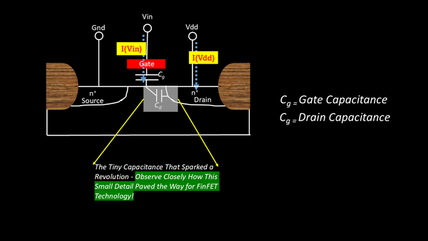
In the race towards smaller, faster, and more efficient transistors, subtle elements like drain capacitance (Cd) have emerged as critical challenges. As shown in the illustration, this tiny capacitance, nestled between the drain and channel, is no longer a minor inconvenience -
it has become a driving force behind the industry's transition to FinFET technology. Let's dive deeper to understand how managing Cd is reshaping the future of semiconductor design.
Understanding Gate and Drain Capacitance in Transistors with SPICE Simulation
Let’s explore the behavior of a transistor when driven by a pulsed input voltage Vin. The
focus lies on how gate-to-channel capacitance (Cg) and drain-to-channel capacitance (Cd) affect the transistor's performance.
Transistor Behavior and Capacitance Impact
In the ideal scenario, only the gate voltage Vin and the capacitance between the gate and channel (Cg) control the transistor's on/off state. However, in real
transistors, the drain voltage Vd influences the channel potential through its associated capacitance Cd. This effect is essential to account for, as it introduces variations in the transistor’s switching characteristics, potentially leading to unintended delays or changes in performance.
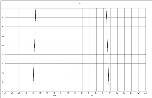
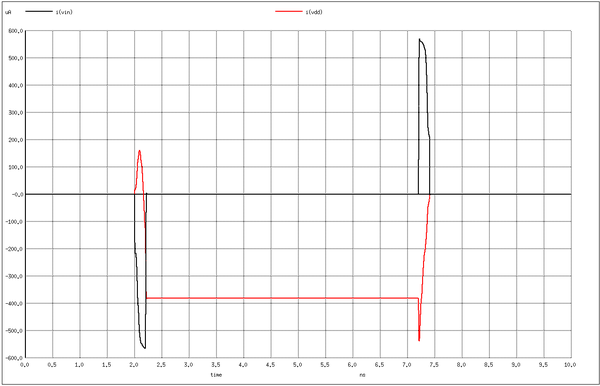
Analyzing the Simulation Graphs
1.
Graph 1: Input Voltage Vinvs Time