Hi
VLSI System Design (VSD) and International Institute of Information Technology Bangalore (IIITB)
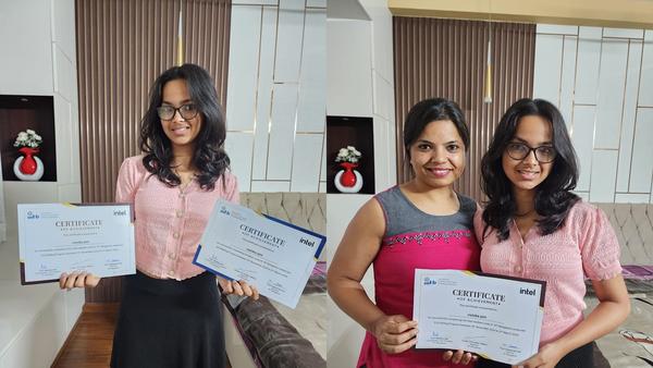
has been impacting LIVES of participants staying in same apartment and never knew about it. This is an example of Rishika Jain, youngest Chip Designer from my tower, 10th Standard girl from Sri Chaitanya Techno School, Bangalore, daughter of Sachin Jain and Parul Jain
Can you imagine? She completed Levels 1 and 2
of the "Chip Design for High School" program while preparing for her board exams, securing 93% in CBSE! This is the level of dedication and passion needed for the future of India's Grand Semiconductor Mission.
The entire VLSI System Design (VSD) is very inspired by the next generation. As a result, all VSD educational products (including boards and semiconductor curriculum) are designed to fit the needs of the upcoming
generation.
Kudos to her parents, who have been an inspiration to Rishika and allowed her to follow her passion.
Below is the program that Rishika and many other school participants completed (Next cohort to be announced soon):
https://www.vlsisystemdesign.com/vlsi-awareness/
The inauguration call recording is
available for all of you to view the format of the program
Upcoming VSD programs (registration closes in last 2 days)
https://www.vlsisystemdesign.com/hdp/