Hi
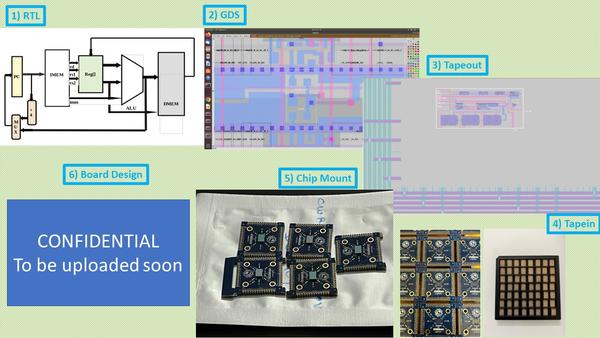
Look at the image and doesn't it look like a dream VLSI program,
where RTL-GDS-Tapeout-Tape In-Chip mounting-Board design is something which every VLSI fresher and professional aspires to witness once in their career? VSD was 100% involved in doing all the above steps for more than 40+ in-house designs and it can't get more exciting than this
It was my dream when I was a student and so we are happy that such a curriculum is a dream come true for everyone. The image shows the reason why different areas of electronics and system design exist in the first place and what it takes to cover all 6 steps shown in the image. The HDP program covers Steps 1) and 2) in detail. But it doesn't stop there. For participants who complete the program 100%, VSD will personally love to engage with
them to complete 3), 4), 5) and 6) for zero additional cost
VSD-HDP program black Friday sales end in 3-days and below is the registration link with more details
Thanks to efabless, Google and Skywater for being the reason for using open-source EDA tools and enabling students to collaborate freely across organizations even after the
course is over as there are no legal agreements to use open-source technology. With the advent of SKY130 PDKs, it enables easy access to tapeout shuttles which are currently sponsored by Google
So all the best and we will see all of you in the HDP program, where you get access to all Udemy courses for
free