Hi
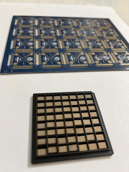
It has been an amazing week for VSD. During Semicon India conference, the hot topic for discussion was semiconductor talent development at scale. VSD has always been of the opinion that trainings and workshops should end at tapeouts and products. There is one thing at the interface - bare dies as you see in the image - which will be packaged as chips. These
chips will then mount over PCB and tested
Now this is quite a moment for VSD and its proud students as we all were dreaming about getting our own chips from our own learning programs. A dream come partially true, as VSD will now go ahead for packaging and testing (hopefully it works)
For VSD community - all your physical design, STA, analog design and physical verification classes and labs are right there in that image. More than 20+ designs yet to be received and you will see what you learnt during VSD-IAT workshops and VSD-HDP hardware design programs
VSD is thankful to its proud community of 80,000+ learners who have been supporting us for more than a decade. All of you WIN today