Hi
Now that you have designed a basic analog circuit from scratch, do you want to go a step ahead and understand how an IP is built from scratch to production?
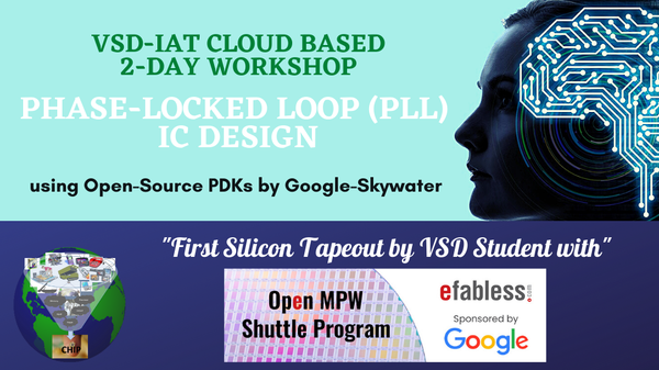
This 2-days workshop on PLL IP design using real Skywater 130nm foundry technology node, focuses exactly those topics - hands-on from Specs to GDS
Here's the link to register:
https://www.vlsisystemdesign.com/pll-design-using-sky130/
Take a look at curriculum and get ready for another exciting cloud lab based hands-on session:
Day 1 – PLL Theory and Lab setup
- Introduction to PLL
- Introduction to Phase Frequency Detector
- Introduction to Charge Pump
- Introduction to VCO and Frequency Divider
- Tool setup and design flow
- Introduction to PDK, specifications and pre-layout circuits
- Circuit design simulation tool - Ngspice Setup
- Layout design tool - Magic Setup
Day 2 – PLL Labs and post-layout simulations
- PLL components circuit design
- PLL components circuit simulations
- Steps to combine PLL sub-circuits and PLL full design simulation
- Troubleshooting steps
- Layout design
- Layout Walkthrough
- Parasitics extraction
- Post Layout simulations
- Steps to combine layouts
- Tapeout theory
- Tapeout labs